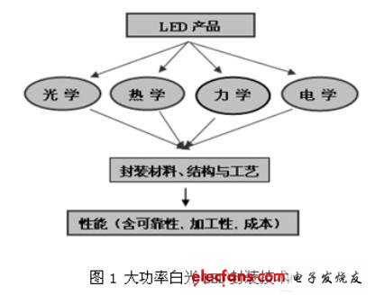
High-power LED packages mainly involve light, heat, electricity, structure and process, as shown in Figure 1. These factors are independent of each other and affect each other. Among them, light is the purpose of LED packaging, heat is the key, electricity, structure and process are the means, and performance is the concrete embodiment of the packaging level. In terms of process compatibility and lower production costs, the LED package design should be carried out simultaneously with the chip design, that is, the package design and process should be considered in the chip design. Otherwise, after the chip is manufactured, the chip structure may be adjusted due to the needs of the package, thereby prolonging the product development cycle and process cost, sometimes even impossible.
Specifically, key technologies for high-power LED packaging include:
First, low thermal resistance packaging process
For the existing LED light effect level, since about 80% of the input power is converted into heat, and the LED chip area is small, the chip heat dissipation is a key problem that the LED package must solve. It mainly includes chip layout, packaging material selection (substrate material, thermal interface material) and process, heat sink design and so on.
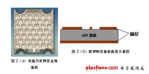
LED package thermal resistance mainly includes internal thermal resistance and interface thermal resistance of materials (heat dissipation substrate and heat sink structure). The function of the heat dissipation substrate is to absorb the heat generated by the chip and conduct it to the heat sink to achieve heat exchange with the outside world. Commonly used heat sink materials include silicon, metals (such as aluminum, copper), ceramics (such as AlN, SiC) and composite materials. For example, Nichia's third-generation LED uses CuW as the substrate, and the 1mm chip is flip-chip mounted on the CuW substrate, which reduces the thermal resistance of the package and improves the luminous power and efficiency. Lamina Ceramics has developed a low-temperature co-fired ceramic metal substrate. , as shown in Figure 2 (a), and developed the corresponding LED packaging technology. The technique first prepares a high-power LED chip suitable for eutectic soldering and a corresponding ceramic substrate, and then directly solders the LED chip to the substrate. Since the eutectic solder layer, the electrostatic protection circuit, the driving circuit and the control compensation circuit are integrated on the substrate, the structure is simple, and the thermal conductivity of the material is high, the thermal interface is small, and the heat dissipation performance is greatly improved, and the high-power LED array package is provided. Proposed a solution. The high thermal conductivity copper-clad ceramic plate developed by Curmilk Company of Germany is made of ceramic substrate (AlN or) and conductive layer (Cu) sintered at high temperature and high pressure. No adhesive is used, so the thermal conductivity is good, the strength is high, and the insulation is strong. , as shown in Figure 2 (b). Among them, aluminum nitride (AlN) has a thermal conductivity of 160 W/mk and a coefficient of thermal expansion (corresponding to the thermal expansion coefficient of silicon), thereby reducing the thermal stress of the package.
Studies have shown that the package interface has a great influence on the thermal resistance. If the interface cannot be processed correctly, it is difficult to obtain a good heat dissipation effect. For example, a well-contacted interface at room temperature may have interfacial gaps at high temperatures, and warpage of the substrate may also affect bonding and local heat dissipation. The key to improving LED packaging is to reduce interface and interface contact thermal resistance and enhance heat dissipation. Therefore, the choice of thermal interface material (TIM) between the chip and the heat sink substrate is important. The TIM commonly used in LED packaging is conductive adhesive and thermal conductive adhesive. Due to the low thermal conductivity, it is generally 0, 5-2, 5W/mK, resulting in high interface thermal resistance. The use of low temperature or eutectic solder, solder paste or conductive paste with nano-particles as the thermal interface material can greatly reduce the interface thermal resistance.
Second, high light extraction rate package structure and process
In the process of using LED, the loss of photon generated by radiation recombination mainly includes three aspects: internal structural defects of the chip and absorption of materials; reflection loss of photons at the exit interface due to refractive index difference; The total reflection loss caused by the incident angle being greater than the critical angle of total reflection. Therefore, a lot of light cannot be emitted from the chip to the outside. By coating a surface of the chip with a relatively high refractive index transparent layer (potting glue), since the glue layer is between the chip and the air, the loss of photons at the interface is effectively reduced, and the light extraction efficiency is improved. In addition, the potting function also includes mechanical protection of the chip, stress release, and as a light guide structure. Therefore, it is required to have high light transmittance, high refractive index, good thermal stability, good fluidity, and easy spraying. In order to improve the reliability of the LED package, the potting compound is also required to have low hygroscopicity, low stress, and aging resistance. Currently used potting compounds include epoxy resin and silica gel. Because of its high light transmittance, large refractive index, good thermal stability, low stress and low hygroscopicity, silica gel is superior to epoxy resin and is widely used in high-power LED packaging, but the cost is high. Studies have shown that increasing the refractive index of silica gel can effectively reduce the photon loss caused by the physical barrier of refractive index and improve the external quantum efficiency, but the performance of silica gel is greatly affected by the ambient temperature. As the temperature increases, the thermal stress inside the silica gel increases, causing the refractive index of the silica gel to decrease, thereby affecting the LED light efficiency and light intensity distribution.
The role of the phosphor is to combine light and color to form white light. Its characteristics mainly include particle size, shape, luminous efficiency, conversion efficiency, stability (heat and chemistry), etc., among which luminous efficiency and conversion efficiency are key. Studies have shown that as the temperature rises, the quantum efficiency of the phosphor decreases, the light emission decreases, and the radiation wavelength also changes, which causes the color temperature and chromaticity of the white LED to change, and the higher temperature accelerates the aging of the phosphor. The reason is that the phosphor coating is prepared by epoxy or silica gel and phosphor, and the heat dissipation performance is poor. When subjected to ultraviolet light or ultraviolet light, temperature quenching and aging are liable to occur, and the luminous efficiency is lowered. In addition, the thermal stability of potting and phosphors at high temperatures is also problematic. Since the common phosphor size is above 1 um, the refractive index is greater than or equal to 1, 85, and the refractive index of the silica gel is generally around 1, 5. Due to the mismatch in refractive index between the two, and the phosphor particle size is much larger than the light scattering limit (30 nm), light scattering exists on the surface of the phosphor particles, which reduces the light extraction efficiency. By incorporating nano-phosphor in silica gel, the refractive index can be increased to 1, 8 or more, light scattering can be reduced, LED light-emitting efficiency can be improved (10%-20%), and light color quality can be effectively improved.
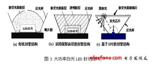
The traditional method of phosphor coating is to mix the phosphor with the potting compound and then apply it to the chip. Due to the inability to accurately control the thickness and shape of the phosphor coating, the color of the emitted light is inconsistent, and blue or yellowish light appears. The Conformal CoaTIng technology developed by Lumileds can achieve uniform coating of phosphors, ensuring uniformity of light color, as shown in Figure 3(b). However, studies have shown that when the phosphor is directly coated on the surface of the chip, the light extraction efficiency is low due to the presence of light scattering. In view of this, the Rensselaer Institute of the United States proposed a Scattered Photon ExtracTIon method (SPE) by placing a focusing lens on the surface of the chip and placing the phosphor-containing glass sheet at a certain position from the chip. Improved device reliability and greatly improved light efficiency (60%), as shown in Figure 3(c).
In general, in order to improve the light-emitting efficiency and reliability of LEDs, the encapsulant layer has a tendency to be gradually replaced by high-refractive-index transparent glass or glass-ceramics, and the phosphor is not only improved by being doped or externally coated on the glass surface. The uniformity of the phosphor and the increase in packaging efficiency. In addition, reducing the number of optical interfaces in the direction in which the LEDs are emitted is also an effective measure to improve the light extraction efficiency.
Retro hanging light is very suitable for Living Room,Dining Room,Study room,Bedroom,Restaurant,Lobby, Bar,Coffe shop and so on.
hanging lamp Retro light is for North America, Southeast Asia, Eastern Europe, Africa(except Middle East), Hong Kong/ Macao/ Taiwan, Latin America, Japan & Korea, Mainland China, Western & Southern Europe, Northern Europe, Central & Southern Asia, Middle East market.
Retro hanging lamp,Retro hanging light,hanging lamp Retro light
Monike lighting , https://www.monikelight.com