The reader is mainly composed of a control unit, a high frequency transceiver module, an antenna, and other interfaces connected to the background device. A transponder, also known as a tag, is the source of RFID reading data and consists primarily of antennas and microelectronic chips. A key part of the RFID system is the reader, and the core technology for implementing the reader is the receiving circuit. This paper mainly analyzes and constructs the UHF passive RFID reader receiving circuit.
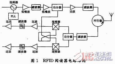
1 Basic architectureThe circuit structure that makes up the RFID reader is shown in Figure 1, with the upper half being the transmit link and the lower half being the receive link.
The reader using the UHF band first implements PIE coding for the baseband signal and implements the 80% to 100% ASK modulation process. In the receiving circuit part, it is necessary to support demodulation in the form of PSK or ASK, and at the same time, Miller or FM0 subcarrier decoding of the baseband signal can be implemented. The system's transmit signal is as follows:
![]()
Where: f(t) represents the signal received by the tag; m(t) represents the baseband signal; carrier frequency is represented by ωc.
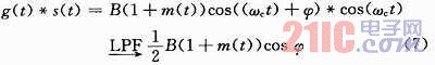
In the label backscattering process, the receiving end receives the following signals:
![]()
Where: g(t) represents the signal received by the receiving end; m'(t) represents the baseband signal of the tag end.
Finally, the down conversion is performed in the receiving circuit, and the demodulation process and results are as follows:
In the formula: ![]() Represents the result of passing the low pass filter.
Represents the result of passing the low pass filter.
The circulator isolation device in Figure 1 typically achieves a 20 to 30 dB isolation. In addition, the use of two independent antennas to receive and transmit tasks, respectively, can also achieve better isolation. It should be noted that in the receiving process, the same frequency carrier must be transmitted at the same time, so the following conclusions can be drawn: the noise in the system is divided into the following types: the surrounding environment interferes with the noise, the transmitting end couples the same frequency leakage at the receiving end and the electron The device's own noise, in addition to the loss between the device interfaces.
According to the radar equation:
![]()
Where: Pr, Pt represent the received and transmitted power respectively; Gt represents the transmit gain; Ar represents the area of ​​the receive antenna; σ represents the cross-sectional area of ​​the radar; Rr, Rt represent the length of the receive and transmit paths, respectively.
Based on the radar equation, a logarithmic form of communication equation can be derived, as follows:
![]()
That is to say, the received power is equal to the sum of the transmit antenna gain, the transmit power, and the receive antenna gain, and then the system loss and the spatial loss are subtracted, so the space loss Lc can be obtained by the following formula:
![]()
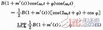
If the unmodulated carrier is f(t)=Acos(ωct), the signal transmitted by the tag is g(t)=B(1+m(t))cos(ωct+φ), and the leakage from the transmitting end to the receiving end of the circulator (ie TX-RX Lea-k) is related to f(t), which is l(t)=Ccos(ωct); s(t)=cos(ωct) represents the clock signal, then l(t),g(t The results after mixing with s(t) are as follows:
![]()
It can be known from the comparison of the power that the coefficient C, that is, the amplitude after TX-RX Leak demodulation is much larger than the amplitude of the label return signal, and can be seen to be a large DC component, so the DC offset generated during the demodulation process Moving is a tricky issue. Therefore, it can be concluded that the peripheral frequency leakage coupled to the receiving end is the most important interference. How to suppress this interference requires further study. There are many methods for suppressing interference, and each solution is not the same. It can be seen from equations (3) and (7) that the signal received by the system has a specific phase difference φ with the clock signal. Since the position of the label is different, cosφ also changes, so in the receiving circuit, the positive Hand over the structure.
2 System Simulation and Theoretical VerificationThe Simulink simulation is implemented to construct the structure of the system transceiver link, as shown in Figure 2. The upper part of Fig. 2 is the tag receiving signal and the transmitting link, and the lower part is the result of superimposing the circulator transmitting and receiving coupling signal and the tag returning signal, and performing the down conversion process at the receiving end. According to the ISO18000-6C protocol standard, the tag return information uses Miller subcarrier modulation or FM0 code modulation, and then ASK modulation is implemented, and the repeated "1101001101" sequence FM0 code is used in the simulation environment. Since the Miller coded or FM0 coded spectrum has a small DC component characteristic, it is filtered out during filtering and the large DC DC drift generated during the downconversion process. If the reader-to-tag distance is 1 m, the calculated spatial loss is 18 dB, where the circulator isolation can be set to 20 dB.
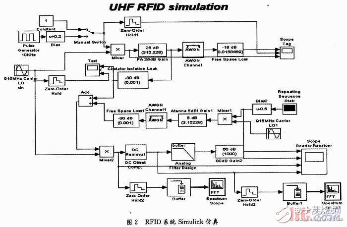
After demodulation by the receiver, the acquired time domain waveform of the label return information is as shown in FIG. 3, and the upper and lower waveforms respectively indicate the baseband information transmitted by the label end, and the information after the receiver demodulates. Figure 4 shows the spectrum of the signal before and after filtering out the DC in the receive chain. The upper picture shows the spectrum of the signal after filtering out DC, while the lower picture shows the spectrum before filtering, which contains a large DC component.
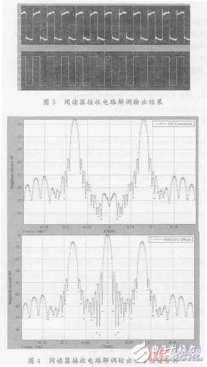
As can be seen in Figure 4, it is necessary to plug in a filter that can filter DC at the back end of the receiver mixer. Since there is no influence on the integrity of the FM0 signal, the system requirements can be met. At the same time, it can be seen that because of the reverse leakage of the circulator, etc., the receiving and receiving interference of the receiving end is relatively large, which is likely to cause the receiver to block.
3 ConclusionIn summary, based on the ISO18000-6C protocol, this paper studies and designs the UHF RFID reader receiving circuit, and implements a theoretical analysis of the zero-IF receiving structure, and analyzes its advantages and disadvantages. Through simulation, the signal waveform and spectrum characteristics of the zero-IF structure are obtained, and it can be seen that it can realize the requirements of the RFID system.
KNL5-63 Residual Current Circuit Breaker
KNL5-63 Moulded Case Circuit Breaker is MCCB , How to select good Molded Case Circuit Breaker suppliers? Korlen electric is your first choice. All moulded Case Circuit Breakers pass the CE.CB.SEMKO.SIRIM etc. Certificates.
Moulded Case Circuit Breaker /MCCB can be used to distribute electric power and protect power equipment against overload and short-current, and can change the circuit and start motor infrequently. The application of Moulded Case Circuit Breaker /MCCB is industrial.
Korlen electric also provide Miniature Circuit Breaker /MCB. Residual Current Circuit Breaker /RCCB. RCBO. Led light and so on .
KNL5-63 Molded Case Circuit Breaker,Small Size Molded Case Circuit Breaker,Electrical Molded Case Circuit Breaker,Automatic Molded Case Circuit Breaker
Wenzhou Korlen Electric Appliances Co., Ltd. , https://www.korlen-electric.com