With the rapid development of integrated circuit technology and the demand for consumer electronic products, especially portable (mobile) customer-oriented electronic products, the rapid development of SoC (System on Chip) has been promoted, and many new ones have been proposed. Question [1]. For a Battery-driven SoC chip, you can no longer just consider two aspects of its optimization space - performance and cost, but must pay attention to the third that it has shown and is becoming more and more important. One aspect - power consumption, in order to extend battery life and electronic product runtime.
The power consumption of CMOS circuits in SoC is as follows: First, static power consumption is mainly caused by static current and leakage current; second is dynamic power consumption, which is mainly caused by transient open circuit current caused by signal conversion in circuit (crowbar current) And the load current and other factors [2], it is the main source of power consumption in SoC chips [3]. Therefore, solving the dynamic power consumption in the SoC is the key to reducing the power consumption of the entire SoC chip. The power consumption mentioned later in this article refers to the dynamic power consumption in the SoC chip.
How to reduce the power consumption in the SoC, different solutions will lead to different solutions. From the perspective of the system level of the chip, there are low-power bus design, low-power storage system design, low-power clock network design, development system rest mode, clock gating and other technologies; from the chip's behavior level ( RTL), there are signal gating, pre-computation, operand separation, state machine optimization, parallel and pipeline structure technology; from the gate level of the chip, there are buffer insertion, extraction factor, unit scaling, Pin switching, phase configuration and other technologies [4]. Considering the power consumption problem from the higher level of abstraction, the magnitude of chip power optimization is more significant.
The SoC low power management based on dynamically configured clocks proposed in this paper is considered from the system level of the chip. In the final experiment, it significantly reduced the power consumption of the entire chip.
1 SoC low power management principle for dynamically configuring clocks
The complexity of SoC design based on microprocessor applications varies greatly: in some applications, all hardware resources may be needed, but in some other applications, only some of the hardware resources may be needed; in some applications It may require a high operating frequency, while in other applications it can greatly reduce the operating frequency. The idea of ​​dynamically managing the SoC system clock is to not only dynamically manage the clock source supply of the SoC internal modules, but also dynamically configure the clock frequency of the SoC system.
Dynamically managing the clock source supply of the SoC internal module is to manage the hardware resources inside the SoC according to different applications. In short, it is the operation of opening and closing internal modules. To turn off a single module, you can set an enable bit for each module and then program the enable bit to turn it off or on. But this is not the best, for two reasons: First, the interface part of each module must be always open, otherwise, the CPU core can not program its internal registers at any time; second, the module enable bit is only Its function operation is turned off, and the clock tree in its module is not turned off, that is, the clock tree in it is still active, and the power consumption caused by the clock tree accounts for a large part of the power consumption of a single module. . In fact, most modules are synchronous systems. All operations of the system are performed under the beat of the clock signal [5]. Turning off the clock source can simultaneously close the module and reduce power consumption.
Dynamically configuring the clock frequency of the SoC system dynamically manages the operating frequency of the system to reduce the power consumption of the SoC without sacrificing system performance. Clock frequency is an important factor affecting dynamic power consumption: [3]. The higher its operating frequency, the greater the power consumption. But in many cases, all modules do not work at the same clock frequency, or the same module can work at different clock frequencies at different times. These are the prerequisites for dynamically configuring the clock frequency of the SoC system.
Figure 1 shows the clock network (clock tree) in the entire SoC. The power management module in the figure does this.
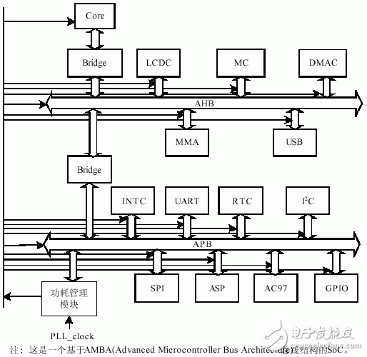
Figure 1 SoC clock network
2 chip low power work management mode
In order to better implement the SoC low-power management strategy of dynamically configuring clocks, the chip has developed four working modes in its low-power management mechanism: Slow, Normal, Idle, and Sleep. The working mechanism of the working mode flow chart shown in FIG. 2 will be described below.
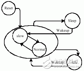
Figure 2 Work mode process
Table 1 shows the status of the four operating modes.
Table 1

(1) Slow mode
The system enters the Slow mode when the system is reset or when the system turns off the PLL and does not require high-speed clock operation. In the Slow mode, the clock core of the CPU core and all modules in the system comes from the crystal oscillator. If the system considers it necessary to turn off some modules, then the clock source enable bit of the corresponding module can be turned off by configuring the internal registers of the power management module.
(2) Normal mode
If you need a high speed clock in some applications, you should switch to Normal mode. In Normal mode, the CPU core in the system and the clock source for all modules come from the PLL. Of course, in this mode, some modules can also be turned off depending on the application of the system. If the system needs to adjust the frequency of the clock, it can be achieved by dynamically configuring the PLL. However, in the process of dynamically configuring the PLL, pay attention to such a problem: because the PLL has a clock lock time, during which time the output clock waveform is irregular, and it cannot be used as the clock source of the chip. In order to ensure the normal operation of the system, the clock source of the system can be temporarily switched to the state of the crystal oscillator, and the clock source of the system is switched to the PLL state after the clock output of the PLL is stabilized.
(3) Idle mode
If the CPU core has processed all tasks in the current state and will be idle for a long time, the system should enter Idle mode. In Idle mode, only the clock source of the CPU core is turned off, and all modules remain as they are. However, in this mode, the PLL cannot be dynamically configured to get different clock frequencies. It is also not possible to dynamically manage the clock source of each module. Because this clock Core has been dormant, it has no way to register the internals of the power management module. Configure it. The system can enter Idle mode regardless of whether the previous state is Slow mode or Normal mode; when the system exits Idle mode, it should fall back to the previous working mode. When the system needs the CPU core to perform transaction processing again, the system can be returned to the Slow mode or the Normal mode by a wake-up signal.
(4) Sleep mode
If the entire system has processed all transactions and will be idle for a long period of time, the system should enter Sleep mode. In Sleep mode, turn off the clock source for the CPU core and all modules. Although it is possible to switch from the Slow mode or the Normal mode to the Sleep mode, when it exits the Sleep mode, the system can only return to the Slow mode. Because in order to further reduce the power consumption of the entire chip, the PLL will be turned off at the same time in the Sleep mode, so it can only return to the Slow mode when it exits, and then decide whether it is necessary to switch to the Normal mode according to the current application. When the system needs to perform transaction processing again, the entire SoC chip system can be woken up by a wake-up signal.
3 power management module implementation
The power management module is mainly composed of a state machine, some multiplexers and some gated clock circuits. The duty of the state machine is to complete the switching between various modes and send out the control signal of the PLL. The multiplexer mainly completes the selection between various clock sources, and the gated clock circuit completes the opening and closing functions of the CPU core and each module clock source. Figure 3 shows the clock source route in the power management module.
As can be clearly seen from Figure 3, two PLLs are illustrated in the power management module: one is the main PLL (MPLL), which provides the clock source for all modules except the USB module in the entire SoC; PLL (UPLL), which only provides a clock source for USB. The MUX completes the selection of the crystal clock and the PLL clock. The selected clock (FCLK) is simultaneously sent to the CPU core, HCLK, and PCLK, and then the clock source is gated according to the needs of each module. This is an SoC based on the AMBA bus structure. According to the AMBA bus protocol, the clock frequency of the CPU core, the module on the AHB, and the module on the APB can be configured in a multiple relationship [6]. The clock source divided by HCLK is only provided to the module on the AHB, and the clock source divided by PCLK is only provided to the module on the APB. AHB_con, APB_con, Core_con, and USB_con manage the clock source supply of the SoC internal modules.
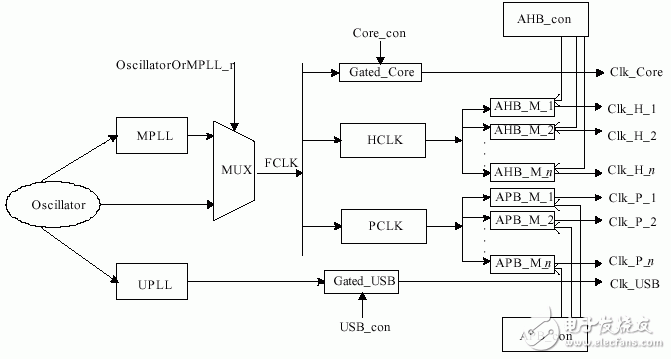
Figure 3 clock source route
4 Problems in dynamic clock management and how to eliminate them
Dynamically configuring the clock frequency of the entire system, although it is convenient to control the power consumption of the entire SoC chip, but also brings some negative effects. Multiplexers and gated clock circuits in the power management unit are most likely to produce glitches, and spurs are fatal to synchronous digital systems. It can lead to failure of synchronization, loss of data, entry of metastability into registers, and, more seriously, failure of the functionality of the entire synchronization system. The glitch is generated because the timing matching of the input signals is problematic, does not appear in the order in which they are set, or the timing of the signal conversion is not appropriate. Therefore, it is necessary to ensure timing matching during RTL design to reduce the possibility of glitch.
There are three situations in the power management module that require a multiplexer:
a. Switch from Slow mode to Normal mode;
b. Reconfigure the PLL in Normal mode;
c. Switch from Normal mode to Slow mode.
Figure 4 is a two-in-one MUX in the power management module. Its control signal is OscillatorOrMPLL, the two selection sources are clk_MPLL and clk_Osci, and the output is out_ClockSource. When the OscillatorOrMPLL is "1", the MUX selects clk_Osci; when the OscillatorOrMPLL is "0", the MUX selects clk_MPLL. The clk_MPLL or clk_Osci must have stabilized before the MUX selects any of these clock signals. To emphasize that stability here does not mean that a complete clock signal has been delivered, but a high or low level is delivered. Thus, when the selector switch reaches their side, it receives a clock signal that is free of glitch and does not operate on the entire SoC. Although the frequency of the SoC is reduced at this time because of this operation, it is temporary (about 2 to 3 crystal clock cycles), so the impact on the overall SoC performance is negligible. The selected signal (clk_MPLL or clk_Osci) is then sent out of the clock signal without glitch, so that the final clock signal is glitch removed.
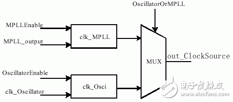
Figure 4 MUX structure
Figure 5 is a timing diagram when the system switches from the Slow mode to the Normal mode. The PLL, the in_PLLStartOrStop signal, is turned on by configuring the internal registers of the power management module, which triggers the Slow2Normal_r signal, indicating that it is currently transitioning from the Slow mode to the Normal mode. Then, this signal triggers the Lock TIme counter to start counting (the count value is determined by the formula given by the PLL's IP provider), then turns off the crystal clock enable signal, and then switches the multiplexer to the MPLL. One party. Finally, the enable signal of the PLL clock is turned on, and the PLL clock that is multiplied is obtained.
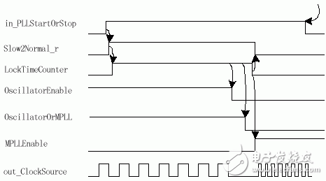
Figure 5 Slow to Normal switching timing
It can be clearly seen from the timing diagram that during the switching of the clock source, the frequency of the finally sent clock (out_ClockSource) will be significantly reduced (about 1/3 or 1/2 of the crystal clock frequency); but if selected The crystal clock frequency above 10MHz will not affect the performance of the entire SoC chip.
As for the gated clock circuit, many people have done extensive research in this area, and this article will not explain this too much [7].
5 Conclusion
This paper presents a low power management strategy for SoC chips. The basic idea is that, first of all, from a global perspective, the clock frequency of the SoC chip is dynamically configured according to various application environments on the premise of satisfying performance. Then, consider a single module separately from the local, and decide whether to turn on its clock source by judging its current working state.
This low-power management solution has been applied to a SoC chip we designed - Garfield. After the Power Compiler power analysis listed in Table 2, it can be clearly seen that the power consumption in the Slow mode is only about 17% of the power consumption in the Normal mode, and the power consumption in the Sleep mode is lower.
Table 2 Power Analysis Results

Non Pressurized With Tubes is one of the Solar Water Heater.Solar water heating (SWH) is heating water by sunlight, using a solar thermal collector. A variety of configurations is available at varying cost to provide solutions in different climates and latitudes. SWHs are widely used for residential and some industrial applications.
Solar Hot Water Tank,Non-Pressure Tubes Solar Water Heater,Solar Water Heater,Solar Water Heater Tubes
NANTONG RONGCHANG IMPORT&EXPORT CO.,LTD , https://www.ergsolarcn.com