Abstract: Multi-core digital signal processors (DSPs) are equipped with a variety of peripheral interfaces, each requiring its own independent reference clock. Due to the high-speed data processing capabilities of multi-core DSPs, the clock requirements for these interfaces are stringent. When multiple interfaces operate simultaneously, precise clock synchronization becomes essential. This paper explores the clock design of the multi-core DSP Ding MS320C6678. The CDCM6208 clock chip is used to provide multiple clock signals at different frequencies to the DSP. The paper details the initialization and configuration of the clock chip, as well as the software and hardware design methods involved.
Introduction
Multi-core processors have become a key trend in modern electronics. These devices integrate multiple similar or heterogeneous processors on a single chip, significantly enhancing computational power. Digital Signal Processors (DSPs) are widely used due to their superior performance in digital signal processing. As an example of high-performance multi-core DSPs, the TMS320C6678 contains eight cores that can operate independently or in parallel. When working together, these cores require efficient communication and handshake mechanisms, especially in time-sensitive applications where clock stability and synchronization are critical. Ensuring stable and synchronized clocks places high demands on system design, including clock sources, distribution, PCB layout, and shielding techniques.
This article discusses the use of the CDCM6208 clock distribution chip to supply multiple clock signals to the C6678 multi-core DSP. These include the core clock, DDR3 read/write clock, RapidIO and PCIe transmission clocks, and Gigabit network accelerator clocks. The paper covers the detailed circuit design, clock chip configuration, and initialization of related on-chip components.
1. C6678 and Its Architecture
The C6678 is an 8-core floating-point DSP from Texas Instruments, capable of operating up to 1.25 GHz. Each core provides 40 GMAC fixed-point or 20 G FLOP floating-point performance. A single chip can deliver up to 320 G MAC or 160 G FLOP of computing power. The internal architecture of the C6678 is illustrated in Figure 1.
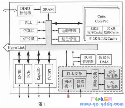
Each core of the C6678 has 32 KB of program memory, 32 KB of data memory, and 512 KB of Level 2 cache. The chip also features a 4 MB shared SRAM. It includes a DDR3 controller interface that supports external DDR3 memory with a maximum addressable range of 8 GB. The C6678 integrates interfaces such as RapidIO, PCIe, EMIF, SPI, and I2C, which communicate through an on-chip high-speed interconnect bus.
The network-related on-chip modules are shown in the gray area at the lower right of Figure 1. These include two SGMII interfaces, Ethernet switching modules, security accelerators, and packet accelerators, enabling fast data detection, verification, and protocol compliance. These modules help discard invalid data, reducing CPU workload. To speed up data exchange between the network and the CPU, the chip uses an on-chip queue manager for packet buffering and distribution, using packet DMA instead of CPU intervention.
Other on-chip components include PLLs, emulation ports, semaphores, power management, and reset management. The PLLs generate the clock for the CPU and peripherals, while the emulation port allows for software monitoring. Semaphores manage task control in the DSP/BIOS OS, and power management controls voltage and current across the chip. Reset management supports both full and partial boot modes.
2. CDCM6208 and Its Structure
The CDCM62xx series, developed by Texas Instruments, is designed for multi-core processors. The CDCM6208, the second-generation chip, offers significant power savings—reducing consumption from 2–3 W in earlier versions to about 0.5 W. Despite this improvement, its functionality, performance, and size remain unchanged. The CDCM6208 has two optional clock inputs and eight output channels. Four of the outputs support integer division, while the other four allow fractional division, meeting diverse clocking needs for multi-core chips. The chip supports LVPECL, CML, HCSL, and LVDS signal levels, with a maximum frequency of 800 MHz for high-speed interfaces like RapidIO and PCIe. Its clock jitter is less than 265 fs, and it can be controlled via SPI or I2S, making it flexible and user-friendly. TI provides a graphical tool for configuration, allowing users to select and set clock modes easily.
Software generates register values based on desired output frequencies, and these are written to the chip via SPI or I2S to complete the configuration.
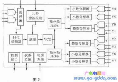
The internal structure of the CDCM6208 is shown in Figure 2. After selecting two input clocks, a 14-fold multiplier is used as a reference to drive the on-chip VCO. To improve phase noise, the multiplied signal passes through an on-chip filter, adjustable via an RC circuit. The VCO clock is divided into two prescalers, which can divide by 4, 5, or 6. After the prescaler, the clock enters a later divider, which includes two fractional dividers and one integer divider. The final output is then driven and sent out. As seen in the right side of Figure 2, the integer dividers Y0 and Y1 produce the same frequency, as do Y2 and Y3. The fractional dividers Y4–Y7 offer more flexibility but reduce power consumption. This configuration meets most multi-core processor needs, especially for TI’s C66 and AK2 series DSPs.
3. Hardware Design
Figure 3 shows the clock requirements for the TMS320C6678 application. The main clock consists of a 100 MHz core clock, which the on-chip PLL locks to a frequency ranging from 700 MHz to 1 GHz. The RapidIO and HyperLink interfaces operate at 312.5 MHz, with multipliers of 4, 8, 10, or 16, resulting in frequencies up to 5 GHz. The HyperLink interface multiplies to 40, 80, 100, or 160, reaching speeds up to 50 GHz.
The PCIe interface and PA_SS network accelerator both use a 100 MHz input, which is internally multiplied to meet interface requirements. The DDR3 clock is 66.667 MHz, multiplied by 20 or 25 to reach 1.333 GHz or 1.666 GHz. Each of these clocks has its own independent PLL circuit, with similar setup procedures. The 25 MHz clock in Figure 3 is dedicated to the Gigabit network, provided by a crystal oscillator. The C6678 also provides a clock output signal, defaulting to 1/6 of the core clock (16.667 MHz), which can be used to monitor the chip’s operation status.
open frame touch screen,multi touch frame,touch screen overlay kit,multi touch overlay kit
Guangdong ZhiPing Touch Technology Co., Ltd. , https://www.zhipingtouch.com