Currently, the terminal devices for CMMB mobile TV applications are primarily smartphones, PMPs, GPS devices, in-car TVs, and PCTVs. These systems share common characteristics such as compact size and strong internal interference. The presence of significant interference can severely impact the performance of CMMB mobile reception. System stability is not only influenced by chip performance, antenna quality, and PCB layout, but also by various external interferences in the environment. Neglecting interference suppression during the design phase often leads to substantial performance degradation. Designing a high-performance CMMB mobile digital TV terminal requires a comprehensive approach that considers multiple factors, which will be explored in detail throughout this article.
Zhuosheng Microelectronics' CMMB receiver chip, MXD0251, integrates a self-developed silicon tuner and demodulator along with a 1.2V LDO. It only requires a 3.3V external power supply, reducing system costs and PCB space. The MXD0251 features a noise figure of less than 3.5dB across the UHF band, a carrier-to-noise ratio of 1.4dB for QPSK 0.5 mode, and superior anti-adjacent-channel interference performance exceeding -50dB. Its analog-to-analog same-channel performance reaches -14dB, while its advanced algorithms ensure excellent co-channel interference resistance. This ensures strong reception sensitivity and robust anti-interference capabilities at the chip level. In many cities, signal frequencies are relatively high, and in some areas, both analog co-channel and adjacent-channel interference are intense. The MXD0251's exceptional interference resistance allows it to maintain stable reception under these complex conditions.
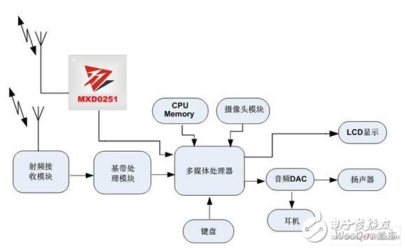
Figure 1: Architecture of the CMMB mobile digital TV terminal system based on MXD0251.
The signal chain begins with the antenna. The most common antennas used in handheld CMMB terminals are whip antennas, ceramic built-in antennas, and active built-in antennas. For example, a whip antenna should ideally be between 120mm and 200mm long, with an optimal length of 180mm. Once the antenna structure is determined, antenna matching is crucial to minimize signal reflection and improve transmission efficiency. For the UHF receive band, it's recommended to include a matching network. A well-matched antenna should have a return loss below -6 dB in the operating band, an average gain greater than -4 dBi, and radiation efficiency over 40%. Post-testing data analysis helps determine if adjustments are needed to achieve conjugate matching or optimize specific frequency bands.
In summary, antenna matching enhances overall performance across the operating band or optimizes specific frequencies. As shown in Figure 2, at 500MHz, the antenna exhibits better resonance and a 5dB gain advantage over 700MHz.
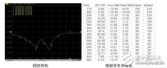
Figure 2: Antenna passive performance.
After selecting the antenna, the RF front end must be carefully designed. On the PCB, RF traces should be as short as possible, avoiding unnecessary bends, digital signals, and non-ground vias. Sufficient RF grounding is essential. Despite these measures, interference may still couple into the RF section. Zhuosheng Microelectronics collaborates closely with leading CMMB antenna manufacturers, helping customers choose the best antenna solution, design effective matching circuits, and conduct antenna tuning together.
Power supply and ground integrity significantly affect the system’s noise floor. Ensuring low power supply ripple is critical. Since CMMB operates in time slots, current fluctuations are expected, requiring careful DC-DC layout to avoid power loop interference. Ground loops should be kept clean and as short as possible, especially in the RF section. If there is strong digital interference, splitting the ground loop can reduce its impact on the RF section.
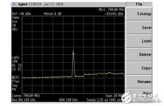
Figure 3: Single tone interference (Span: 20MHz).
System clocks, ADC/DAC, DDR clocks, and certain signal lines can generate spurs at specific frequency points, as seen in Figure 3. At 700MHz, the interference reaches -89dBm, degrading sensitivity at 698MHz. Multiple spurs within the CMMB band can affect several frequencies, as illustrated in Figure 4.
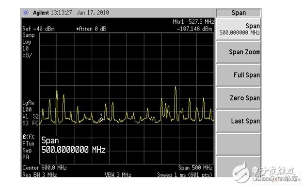
Figure 4: Multiple tone interference (Span: 500MHz).
The MXD0251 includes internal algorithms to detect and filter out spurs. While these issues can often be avoided through proper layout, it's important to keep interference sources away from the RF section. Ground loops should isolate the RF part from digital interference, and any interference paths should be minimized. Each system may face different challenges, so thorough analysis is necessary. Figure 5 shows a system with excellent spur performance, where no spurs appear in the band, resulting in a flat sensitivity curve.
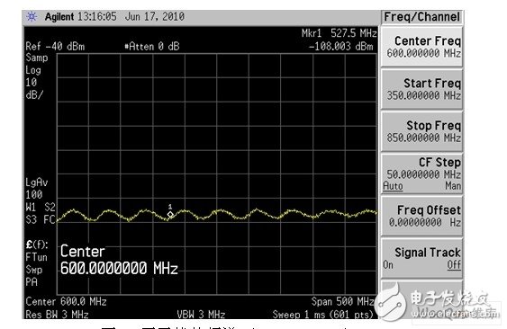
Figure 5: Interference-free spectrum (Span: 500MHz).
Common coupled interferences include radiated interference from LCD FPCs, backlight interference from keyboards, and DC-DC switching. LCDs are typically the main source of interference, with noise coupling into the chip via the antenna, affecting reception performance and often impacting a broader frequency range. Shielding and grounding of signal lines are usually required. In many cases, screen FPCs cause 3–7dB of degradation below 600MHz, with lower frequencies being more affected. Additionally, suppressing other wireless signals in the space is essential, and adding a SAW filter is an effective solution.
In terms of coupled receiving sensitivity, good systems can differ from poor ones by tens of dB, directly influencing the success or failure of a mobile TV product. Zhuosheng Microelectronics offers closed-loop and open-loop performance testing for customer prototypes, identifying potential coupling interference in the entire system. We help locate interference sources, analyze contributing factors, propose suppression strategies, and debug the final product to ensure excellent performance.
High Frequency Inverter,Dc To Ac Inverter,Residential Energy Storage Inverter
Bosin Power Limited , https://www.bosinsolar.com