As the amount of social information increases, people have higher and higher requirements for multimedia video compression. "High compression, low bit rate" high-definition video compression has been widely used in household appliances, medical equipment, military reconnaissance, satellite remote sensing and other fields . The latest ADV212 from ADI is a device with real-time compression / decompression standard (SD) video signal and high-definition (HDTV) video signal function. It has the advantages of good reliability, flexible configuration, and support for various video formats. It is applicable Data processing for multiple video formats. This article introduces the design scheme based on the ADV212 high-definition video compression system, which can support SMPTE274M (1080i) video real-time encoding.
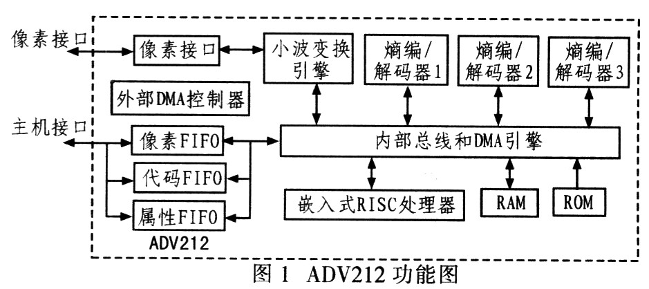
1 ADV212 codec principle Figure 1 shows the functional diagram of ADV212, which is mainly composed of pixel interface, wavelet transform engine, entropy encoder / decoder, embedded RISC processor, memory system and internal and external DMA. The basic process of operation is that video or pixel data is input through the ADV212 pixel interface, and the effective sample value is transmitted to the wavelet transform engine through interlaced scanning (the wavelet transform engine can perform up to 6 levels of wavelet decomposition on the code block). The data entering the wavelet transform engine is divided into tiles or frames, each tile or frame will be decomposed into many sub-bands through 5/3 fixed-point arithmetic or 9/7 floating-point arithmetic filters, and corresponding wavelet coefficients are generated, and then Write to internal register. Three entropy encoders / decoders are used to perform background modeling and arithmetic coding on the coding blocks of wavelet coefficients, and calculate the optimal rate and distortion during the compression process. The data stream of JPEG2000 standard formed by entropy coding is stored in the code FIFO. The code FIFO mainly buffers the internal high-speed bus and low-speed host interface. Stream data can be accessed through a common read and write access protocol ( ![]() , ADDR) output from the host interface, or through the external DMA engine coordinated by the external DMA controller through the DREQ / DACK protocol. The internal DMA engine performs high-bandwidth, high-performance transfers between memories and between modules and memories. The RISC processor has ROM and RAM corresponding to each program and data memory, interrupt controller, standard bus interface and timer counter.
, ADDR) output from the host interface, or through the external DMA engine coordinated by the external DMA controller through the DREQ / DACK protocol. The internal DMA engine performs high-bandwidth, high-performance transfers between memories and between modules and memories. The RISC processor has ROM and RAM corresponding to each program and data memory, interrupt controller, standard bus interface and timer counter.
2 Unified hardware design As a high-definition video data compression system, this solution is first considered from the perspective of system implementation functions and cost performance, using FPGA + ADV212.
Video decoder selection: The video decoder uses the ADV7402 high-definition video decoder. It uses 10-bit ADC, 12 analog inputs, supports standard definition (480i, NTSC, PAL, SECAM), high-definition (1080i, 720p) and graphic RGB input (1 280xl 024 @ 60 Hz), which can be seamlessly connected with ADV212.
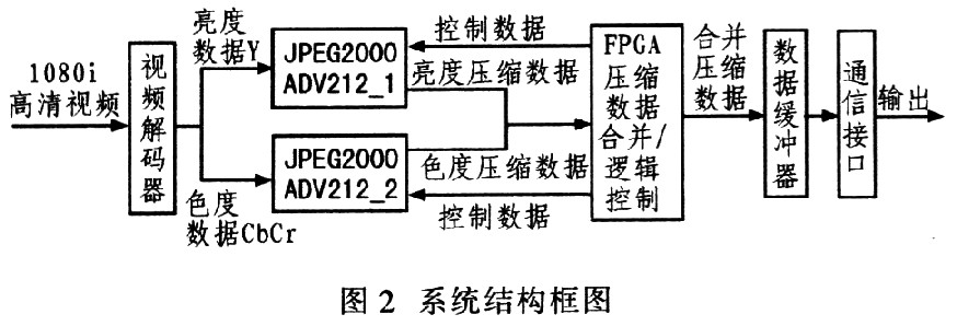
The number of ADV212 pieces is selected: a 10-bit high-definition (HDTV) video signal, the input data transmission rate is about 124 Ms / s, and the input rate limit of the ADV212 pixel interface is 65 MS / s in irreversible mode, reversible mode The following is 32 MS / s. This requires the system to be composed of at least two ADV212. This system selects two ADV212 compression devices. The YCbCr data is formatted in 4: 2: 2, and the data compression processing of brightness (Y) and chrominance (CbCr) is completed. Data use is EAV / SAV encoding format. Figure 2 shows a block diagram of the system structure. This solution includes a video acquisition and decoding module, a video image JEPG200 compression module, a compression merge module, a logic control module, and a communication output module.
FPGA selection: Choose Altera's CycloneIII series EP3C55F484C8 device, which has 328 user I / O, 55,856 available logic elements, 312 embedded multiplier units and 4 phase-locked loops, which can easily realize ADV212 initialization and data compression Capturing and merging of luma compressed data and chroma compressed data.
3 ADV212 device initialization process and parameter configuration
3. 1 ADV212 initialisation procedure The ADV212 initialisation procedure configures the internal direct register and the indirect register of the ADV212 according to the specific instruction command to complete. Figure 3 shows the ADV212 code initialization process. The initialization procedure starts from the access of direct registers such as PLL register, BOOT register, MMODE register and BUSMODE register. When accessing the direct register, the target system must maintain the input pin ADDR. ![]() , And HDATA (write) status. After loading the firmware and configuration parameters, the software restarts, and then configures the BUSMODE and MMODE registers and application-specific registers again. Next, make sure that the correct firmware is loaded by the application ID. The correct firmware loading can be confirmed by the interrupt or voting procedure of the EIRQFLG register. When you are sure that the firmware is loaded and the EIRQFLG register is cleared. Encoding begins.
, And HDATA (write) status. After loading the firmware and configuration parameters, the software restarts, and then configures the BUSMODE and MMODE registers and application-specific registers again. Next, make sure that the correct firmware is loaded by the application ID. The correct firmware loading can be confirmed by the interrupt or voting procedure of the EIRQFLG register. When you are sure that the firmware is loaded and the EIRQFLG register is cleared. Encoding begins.
3. 2 ADV212 parameter configuration Clock configuration: High-definition video 1080i requires VCLK of 74.25 MHz. According to the ADV212 data sheet, JCLK must be at least 2VCLK, so the maximum pulse frequency is recommended to be 0.35J-CLK, which is close to 50 MHz, which is the maximum read and write pulse frequency.
Bus and DMA configuration: When HDTV (1080i) is used, two ADV212 must work in the irreversible maximum transmission rate of 65 MS / s mode, video input adopts 32-bit VDATA bus (pixel interface), compressed data output adopts 2 ADV212 sharing 32 Bit HDATA bus (host interface). Initialize ADV212 to select attribute type 5 (ATTRTYPE), the attribute data reading adopts single transmission DREQ / DACK DMA mode, and the code stream reading adopts pulse transmission DREQ / DACK DMA mode.

As shown in Figure 3. According to the ADV212 direct register configuration, set the ADV212 internal clock, bus mode, indirect register access mode, etc. The initialization process of ADV212_l and ADV212_2 is described as follows: PLL_HIOx008h, PLL_HO, 0x0084: set VCLK to 74.25 MHz; BOOT: 0x008A boot mode is used to load or not; BUSMODE: 0x000A sets the host control data width and DMA data width to 32 bits; MMODE: 0x000A sets the number of indirect data access bits and indirect address step size to 32 bits; IADDR: Ox00050000 sets the starting point of program storage; IDATA: 0x ******** loads the program in the program memory; BOOT Ox008D software Restart; BUSMODE0x000A resets the host control data width and DMA data width to 32 bits: MMODE 0x000A resets the indirect data access bits and indirect address step size to 32 bits. The parameters of ADV212 are set according to IADDR and IDATA. The parameter configuration is described as follows: IADDR 0x00057F00 The starting address of the encoding parameters of ADV212_1 and ADV212_2; IDATA 0x02010503 (ADV212_1), 0x03010503 (ADV212_2) 02 = 1080i brightness (03 = 1080i chroma); 0l = 10-bit precision; 05 = 5-level wavelet transform; 03 = Y, C single-level; IDATA 0x03000000 03 = code block size is 128x32; 00 = irreversible 9x7 wavelet; 00 = skip no byte area; 00 = no attribute data output ; IDATA0x01019500 (ADV212_1), 0x01008700 (ADV212_2) Ol = target video domain, frame size; 019500 = 10: 1 compression ratio (008700 = 30: 1 compression ratio); IDATA 0x00000001 00 = LRCP series format; 00 = EAV. SAV coding, all cathodes are synchronized; 00 = Qfaetor is 1X; 01 = coding format is. j2c; IDATA0x00000000 saves the parameters.
After the above configuration is completed, EIRQFLG (address Ox6h) of ADV212_1 and ADV212_2 is written to 0x0400 to clear the software interrupt (SEIRQ0) and start the program. When DREQ0 becomes valid, ADV2-12 is ready to transmit data from the CODE FIFO. The host follows the specific timing instructions for ADV212 Start data transfer.
4 FPGA structure and function Figure 4 is the internal logic of FPGA. FPGA is mainly composed of the following functional modules: 1) Host logic, Nios-based embedded host logic module, mainly implements 2 ADV212 read and write operations, to achieve the initialization and ADV212 Firmware download; 2) ADV212 arbitration logic, to realize the synchronization of 2 pieces of ADV212 compressed data, answer signal function to answer the bus judgment status; 3) Y / C merge logic, this part realizes the brightness compression data and according to the read attributes and code information Combine function of chroma compression data; 4) Data buffer control module, buffer the data flow between external DMA channel read rate and brightness / chroma merge logic modules.
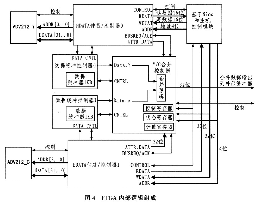
In the FPGA main control module, to ensure that the ADV212 is loaded with the correct firmware, it is implemented in 4 steps: the first step is to write 0x0400 to the external interrupt enable register to mask the software interrupt 0 bit: the second step waits for the interrupt Pin IRQ is pulled low. Step 3 checks whether the EIRQFlLG [10] bit of the external interrupt flag register is set. Step 4 reads the application identifier from the software flag register. If it reads 0XFF82, it means that the firmware is loaded correctly. The system can start working.
When the system starts to work, FPGA is in arbitration. The control module analyzes and judges the number of partition bytes read from the ADV212 attribute FIFO. The data buffer control module registers the compressed data read from the ADV212 code FIFO. The arbitration / control module analyzes the results to control the brightness / chroma merge logic module. The code stream starts from the Y data and merges from the opposite parts of the two devices (Y and CbCr), and is output to the buffer and then output by the communication port.
5 Conclusion The high-definition video compression system based on FPGA + ADV212 structure can realize the real-time processing of high-definition video (YCbCr 4: 2: 2 format) signals. This system has the advantages of high cost performance, good reliability, flexible adjustment, and easy recovery of compressed signals. But this system uses irreversible 9/7 wavelet transform, video processing has certain distortion, in order to obtain 1080i video signal with better characteristics (such as lossless compression), it is recommended to use 3 or more ADV212 to process the signal, The signal format can adopt YCbCr 4: 4: 4 format. With the wide application of JPEG2000, the dedicated image compression device ADV212 will be increasingly used in the field of video and image compression.
RCCB named Residual Current Circuit Breaker. When there is human electricity shock or if the leakage current of the line exceeds the prescribed value, Residual current Circuit Breaker/RCCB(without over-current protection) will cut off the power rapidly to protect human safety and prevent the accident due to the current leakage. The rccb switch which made from Korlen electric can be used as infrequent changeover of the line in normal situation.
Korlen electric ---- the rccb switch manufacturer,produces types of Residual Current Circuit Breaker. It is applicable to industrial site, commercial site, tall building and civil house.
Residual Current Circuit Breaker
Residual Current Circuit Breaker,Ac Residual Current Circuit Breaker,Miniature Residual Current Circuit Breaker,Residual Current Electrical Circuit Breaker
Wenzhou Korlen Electric Appliances Co., Ltd. , https://www.korlenelectric.com