The increase in the functionality of mobile phones has become increasingly demanding on PCB design. With the arrival of a round of Bluetooth devices, cellular phones and the 3G era, engineers are paying more and more attention to the design techniques of RF circuits.
This article refers to the address: http://
Radio frequency (RF) board design is often described as a "black art" because of its many theoretical uncertainties, but this view is only partially correct. RF board design also has many guidelines that should be followed and should not Neglected rules. However, in practical design, the really practical technique is how to compromise these guidelines and rules when they cannot be accurately implemented due to various design constraints. Of course, there are many important RF design topics worth discussing, including impedance and impedance matching, insulation materials and laminates, as well as wavelengths and standing waves, so these have a great impact on the EMC and EMI of mobile phones. Summarize the conditions that must be met when designing the RF layout:
3.1 Separate the high-power RF amplifier (HPA) from the low-noise amplifier (LNA) as much as possible. Simply put, the high-power RF transmit circuit is kept away from the low-power RF receive circuit. There are many functions of mobile phones and many components, but the PCB space is small, and the design process of the wiring is considered to be the highest, and all of these requirements for design techniques are relatively high. At this point it may be necessary to design a four- to six-layer PCB so that they work alternately instead of working at the same time. High power circuits can sometimes also include RF buffers and voltage controlled oscillators (VCOs). Make sure that there is at least one whole piece of high power area on the PCB. It is better to have no vias on it. Of course, the more copper is, the better. Sensitive analog signals should be as far away as possible from high-speed digital and RF signals.
3.2 Design partitions can be broken down into physical partitions and electrical partitions. Physical partitioning mainly involves component layout, orientation, and shielding; electrical partitioning can continue to be broken down into partitions for power distribution, RF traces, sensitive circuits and signals, and grounding.
3.2.1 We discuss physical partitioning issues. Component layout is the key to achieving an excellent RF design. The most effective technique is to first fix the components on the RF path and adjust their orientation to minimize the length of the RF path, keeping the input away from the output and as far as possible. Ground high power circuits and low power circuits.
The most efficient method of board stacking is to arrange the main ground plane (main ground) in the second layer below the surface and walk the RF lines as far as possible on the surface. Minimizing the via size on the RF path not only reduces path inductance, but also reduces the number of solder joints on the primary ground and reduces the chance of RF energy leaking into other areas of the laminate. In physical space, linear circuits like multistage amplifiers are usually sufficient to isolate multiple RF regions from each other, but duplexers, mixers, and IF amplifiers/mixers always have multiple RF/IFs. The signals interfere with each other, so care must be taken to minimize this effect.
3.2.2 RF and IF traces should be crossed as much as possible, and as far as possible between them. The correct RF path is very important for the performance of the entire PCB board, which is why the component layout is usually the majority of the time in the design of the mobile phone PCB. In the design of mobile phone PCB board, it is usually possible to place the low noise amplifier circuit on one side of the PCB board, while the high power amplifier is placed on the other side, and finally connect them to the RF side and baseband processing on the same side through the duplexer. On the antenna of the device. Some tricks are needed to ensure that the straight through hole does not transfer RF energy from one side of the board to the other. A common technique is to use blind holes on both sides. The adverse effects of straight through holes can be minimized by arranging straight through holes in areas where both sides of the PCB are free of RF interference. Sometimes it is not possible to ensure adequate isolation between multiple circuit blocks. In this case, it is necessary to consider shielding the RF energy in the RF area with a metal shield. The metal shield must be soldered to the ground and must be kept with the components. A proper distance, so it takes up valuable PCB space. It is very important to ensure the integrity of the shield as much as possible. The digital signal line entering the metal shield should be as far as possible inside the layer, and it is better that the PCB below the trace layer is the ground layer. The RF signal line can go out from the small notch at the bottom of the metal shield and the wiring layer at the ground notch, but the ground around the notch should be as much as possible, and the ground on different layers can be connected through multiple vias. .
3.2.3 Proper and effective chip power supply decoupling is also very important. Many RF chips with integrated linear circuitry are very sensitive to power supply noise. Typically, each chip requires up to four capacitors and an isolated inductor to ensure that all power supply noise is filtered out. An integrated circuit or amplifier often has an open-drain output, so a pull-up inductor is required to provide a high-impedance RF load and a low-impedance DC supply. The same principle applies to decoupling the inductor's power supply. Some chips require more than one power supply to work, so you may need two or three sets of capacitors and inductors to decouple them separately. The inductors are rarely tied together in parallel because this creates an air core transformer and induces interference with each other. Signals, so the distance between them must be at least equal to the height of one of the devices, or arranged at right angles to minimize their mutual inductance.
3.2.4 The electrical partitioning principle is generally the same as the physical partition, but it also contains some other factors. Some parts of the phone use different operating voltages and are controlled by software to extend battery life. This means that the phone needs to run multiple power supplies, which brings more problems to the isolation. The power supply is typically introduced from the connector and immediately decoupled to filter out any noise from outside the board and then distribute it after passing through a set of switches or regulators. The DC current of most circuits on the PCB board is quite small, so the trace width is usually not a problem. However, it is necessary to separate a large current line as wide as possible for the power supply of the high power amplifier to minimize the transmission voltage drop. . To avoid too much current loss, multiple vias are required to transfer current from one layer to another. In addition, if the high power amplifier's power pin is not fully decoupled, high power noise will radiate across the board and cause a variety of problems. The grounding of high power amplifiers is critical and often requires a metal shield. In most cases, it is also critical to ensure that the RF output is kept away from the RF input. This also applies to amplifiers, buffers and filters. In the worst case, if the outputs of the amplifier and buffer are fed back to their inputs with the appropriate phase and amplitude, they are likely to generate self-oscillation. In the best case, they will work stably under any temperature and voltage conditions. In fact, they can become unstable and add noise and intermodulation signals to the RF signal. If the RF signal line has to be wound back from the input of the filter, this can seriously damage the bandpass characteristics of the filter. In order to get good isolation between the input and the output, it is first necessary to make a circle around the filter, and then the lower layer of the filter is also grounded and connected to the main ground surrounding the filter. It is also a good idea to keep the signal lines that need to pass through the filter as far as possible from the filter pins.
In addition, the grounding of each part of the board should be very careful, otherwise a coupling channel will be introduced. Sometimes you can choose to go single-ended or balanced RF signal lines. The same principles for cross-interference and EMC/EMI apply here. Balanced RF signal lines can reduce noise and crosstalk if the traces are correct, but their impedance is usually high, and a reasonable linewidth is required to get a matching source, trace, and load impedance. Actual wiring may be There will be some difficulties. The buffer can be used to improve isolation because it splits the same signal into two parts and drives different circuits. In particular, the local oscillator may require a buffer to drive multiple mixers. When the mixer reaches the common mode isolation state at the RF frequency, it will not work properly. The buffers are well isolated to isolate impedance changes at different frequencies so that the circuits do not interfere with each other. Buffers are very helpful in design, they can be followed by the circuit that needs to be driven, so that the high power output traces are very short, because the buffer input signal level is relatively low, so they are not easy to the other on the board. The circuit causes interference. Voltage-controlled oscillators (VCOs) convert varying voltages into varying frequencies. This feature is used for high-speed channel switching, but they also convert small amounts of noise on the control voltage into small frequency changes, which gives The RF signal adds noise.
3.2.5 To ensure that no noise is added, it must be considered from the following aspects: First, the expected bandwidth of the control line may range from DC to 2 MHz, and it is almost impossible to remove such wide-band noise by filtering; secondly, VCO The control line is usually part of a feedback loop that controls the frequency. It can introduce noise in many places, so the VCO control line must be handled very carefully. Make sure that the ground underneath the RF trace is solid and that all components are firmly connected to the main ground and isolated from other traces that may cause noise. In addition, to ensure that the VCO's power supply is fully decoupled, since the VCO's RF output tends to be a relatively high level, the VCO output signal can easily interfere with other circuits, so special attention must be paid to the VCO. In fact, the VCO is often placed at the end of the RF area, and sometimes it requires a metal shield. Resonant circuits (one for the transmitter and one for the receiver) are related to the VCO, but they also have their own characteristics. Simply put, the resonant circuit is a parallel resonant circuit with a capacitive diode that helps set the VCO operating frequency and modulate the speech or data onto the RF signal. The design principles of all VCOs also apply to resonant circuits. Resonant circuits are typically very sensitive to noise because they contain a significant number of components, a wide distribution area on the board, and typically operate at a very high RF frequency. The signals are usually placed on adjacent pins of the chip, but these signal pins need to work with relatively large inductors and capacitors to work, which in turn requires that these inductors and capacitors must be placed close together and connected back. A control loop that is sensitive to noise. It is not easy to do this.
An automatic gain control (AGC) amplifier is also a problem that is prone to problems, and both the transmit and receive circuits have an AGC amplifier. AGC amplifiers typically filter out noise effectively, but because handsets have the ability to handle the rapid changes in transmit and receive signal strength, AGC circuits are required to have a fairly wide bandwidth, which makes it easy to introduce AGC amplifiers on critical circuits. noise. Designing AGC lines must follow good analog circuit design techniques, which are associated with very short op amp input pins and very short feedback paths, both of which must be kept away from RF, IF, or high-speed digital signal traces. Also, good grounding is essential and the chip's power supply must be well decoupled. If it is necessary to take a long line at the input or output, then it is better at the output, usually the impedance of the output is much lower, and it is not easy to induce noise. Generally, the higher the signal level, the easier it is to introduce noise into other circuits. In all PCB designs, it is a general principle to keep digital circuits as far away as possible from analog circuits. It is also applicable to RF PCB designs. Common analog grounds and grounds used to shield and separate signal lines are usually equally important, so careful planning, thoughtful component placement, and thorough layout evaluation are important in the early stages of design, and RF lines should also be used. Keep away from analog lines and some critical digital signals. All RF traces, pads, and components should be filled with as much copper as possible and connected to the main ground as much as possible. If the RF traces must pass through the signal lines, try to lay a layer of ground connected to the main ground along the RF traces between them. If this is not possible, make sure they are crisscrossed, which minimizes capacitive coupling while spreading as much ground as possible around each RF trace and connecting them to the main ground. In addition, minimizing the distance between parallel RF traces minimizes inductive coupling. A solid monolithic ground plane is best placed directly on the first layer below the surface, although other practices are useful when designing with care. On each layer of the PCB, place as much ground as possible and connect them to the main ground. Try to keep the traces together to increase the number of plots in the internal signal layer and power distribution layer, and adjust the traces so that you can connect the ground vias to the isolated plots on the surface. Free ground should be avoided on each layer of the PCB because they pick up or inject noise like a small antenna. In most cases, if you can't connect them to the main land, then you'd better remove them.
3.3 When designing the mobile phone PCB board, the following aspects should be given great attention.
3.3.1 Power and Ground Processing
Even if the wiring in the entire PCB board is completed well, the interference caused by the inconsistency of the power supply and the ground line may degrade the performance of the product, and sometimes even affect the success rate of the product. Therefore, the wiring of electricity and ground wire should be taken seriously, and the noise interference generated by electricity and ground wire should be minimized to ensure the quality of the product. For every engineering engineer engaged in the design of electronic products, the reason for the noise between the ground and the power line is understood. Only the reduced noise suppression is described:
(1) It is well known to add a decoupling capacitor between the power supply and the ground.
(2), try to widen the power supply, ground line width, preferably the ground line is wider than the power line, their relationship is: ground line > power line > signal line, usually the signal line width is: 0.2 ~ 0.3mm, the most The fine width can reach 0.05~0.07mm, and the power cord is 1.2~2.5mm. For the PCB of the digital circuit, a wide ground wire can be used to form a loop, that is, a ground net is used for use (the ground of the analog circuit cannot be used in this way)
(3) Use a large-area copper layer for grounding, and connect the unused areas to the ground on the printed board for grounding. Or make a multi-layer board, power supply, ground line each occupy a layer.
3.3.2 Co-processing of digital circuits and analog circuits
Many PCBs are no longer single-function circuits (digital or analog circuits), but rather a mixture of digital and analog circuits. Therefore, it is necessary to consider the mutual interference between them when wiring, especially the noise interference on the ground. The frequency of the digital circuit is high, and the sensitivity of the analog circuit is strong. For the signal line, the high-frequency signal line is as far as possible away from the sensitive analog circuit device. For the ground line, the whole human PCB has only one node to the outside, so The number of processing and the common ground must be handled inside the PCB, and the digital ground and the analog ground inside the board are actually separated from each other, but only at the interface where the PCB is connected to the outside (such as a plug). The digital ground is slightly shorted to the analog ground. Please note that there is only one connection point. There is also no common ground on the PCB, which is determined by the system design.
3.3.3 Signal wires are laid on the electrical (ground) layer
In the wiring of multi-layer printed boards, since there are not many lines left in the signal line layer, the addition of layers will cause waste and increase the workload for production, and the cost will increase accordingly. To resolve this contradiction, consider wiring on the electrical (ground) layer. The power layer should be considered first, followed by the ground layer. Because it is best to preserve the integrity of the formation.
3.3.4 Treatment of connecting legs in large-area conductors
In a large area of ​​grounding (electricity), the legs of common components are connected to them, and the treatment of the connecting legs needs to be comprehensively considered. In terms of electrical performance, the pads of the component legs are perfectly connected with the copper surface, but There are some hidden dangers in the soldering assembly of the components. For example, 1 welding requires a high-power heater. 2 is easy to cause a virtual solder joint. Therefore, taking into account the electrical performance and process needs, making a cross-shaped pad, called heat shield, commonly known as thermal pad (Thermal), so that the possibility of creating a solder joint due to the cross-distribution heat during soldering Sex is greatly reduced. The treatment of the grounding (ground) leg of the multilayer board is the same.
3.3.5 The role of the network system in the wiring
In many CAD systems, cabling is determined by the network system. The mesh is too dense, although the path is increased, but the stepping is too small, the data volume of the field is too large, which inevitably has higher requirements on the storage space of the device, and the computing speed of the object computer electronic product is also Great impact. Some of the paths are invalid, such as occupied by the pads of the component legs or occupied by the mounting holes and the holes. The grid is too sparse, and too few paths have a great impact on the routing rate. Therefore, there must be a sparse and reasonable grid system to support the wiring. The distance between the legs of the standard components is 0.1 inches (2.54mm), so the basis of the grid system is generally set to 0.1 inches (2.54 mm) or less than 0.1 inches of multiples, such as: 0.05 inches, 0.025 inches, 0.02 Inches and so on.
3.4 The techniques and methods for high frequency PCB design are as follows:
3.4.1 The corner of the transmission line should be at a 45° angle to reduce the return loss.
3.4.2 High-performance insulated circuit boards with tightly controlled insulation constant values. This method facilitates efficient management of the electromagnetic field between the insulating material and adjacent wiring.
3.4.3 Improve PCB design specifications for high precision etching. Consider a total line width error of +/- 0.0007 inches, manage the undercut and cross-section of the wiring shape, and specify the wiring sidewall plating conditions. Overall management of the wiring (wire) geometry and coating surface is important to address the skin effect issues associated with microwave frequencies and to implement these specifications.
3.4.4 There is a tapped inductor in the protruding leads. Avoid using leaded components. In high frequency environments, it is best to use surface mount components.
3.4.5 For signal vias, avoid using a via processing (pth) process on sensitive boards because this process can result in lead inductance at the vias.
3.4.6 To provide a rich ground plane. These ground planes are connected using molded holes to prevent the effects of 3-dimensional electromagnetic fields on the board.
3.4.7 To select electroless nickel plating or immersion gold plating, do not use the HASL method for plating. This plated surface provides a better skin effect for high frequency currents (Figure 2). In addition, this high solderable coating requires fewer leads and helps reduce environmental pollution.
3.4.8 Solder mask prevents the flow of solder paste. However, due to the uncertainty of thickness and the unknown nature of the insulation properties, covering the entire surface of the board with the solder resist material will result in a large change in the electromagnetic energy in the microstrip design. A solder dam is generally used as a solder mask. Electromagnetic field. In this case, we manage the conversion between the microstrip and the coaxial cable. In a coaxial cable, the ground plane is annularly interlaced and evenly spaced. In the microstrip, the ground plane is below the active line. This introduces some edge effects that need to be understood, predicted, and considered at design time. Of course, this mismatch can also cause return loss, which must be minimized to avoid noise and signal interference.
3.5 Electromagnetic compatibility design
Electromagnetic compatibility refers to the ability of an electronic device to work in a coordinated and efficient manner in various electromagnetic environments. The purpose of the electromagnetic compatibility design is to enable the electronic device to suppress various external interferences, enable the electronic device to work normally in a specific electromagnetic environment, and at the same time reduce the electromagnetic interference of the electronic device itself to other electronic devices.
3.5.1 Choosing a reasonable wire width
Since the transient interference generated by the transient current on the printed wiring is mainly caused by the inductance component of the printed conductor, the inductance of the printed conductor should be minimized. The inductance of a printed conductor is proportional to its length and inversely proportional to its width, so that short and precise conductors are advantageous for suppressing interference. Signal lines for clock leads, row drivers, or bus drivers often carry large transient currents, and the printed conductors should be as short as possible. For the discrete component circuit, when the width of the printed conductor is about 1.5mm, the requirement can be fully satisfied; for the integrated circuit, the width of the printed conductor can be selected between 0.2 and 1.0mm.
3.5.2 Adopting the correct routing strategy
The use of equal traces can reduce the wire inductance, but the mutual inductance and distributed capacitance between the wires increase. If the layout allows, it is better to use a well-shaped mesh wiring structure. The specific method is that one side of the printed board is laterally routed, and the other side is longitudinally routed. Metallized holes are then connected at the intersection holes.
3.5.3 In order to suppress the crosstalk between the printed circuit board wires, the long distance equalization should be avoided when designing the wiring. Pull the distance between the wires and the wires as much as possible. The signal wires and ground wires and power cables should be as far as possible. Do not cross. A grounded trace is placed between some signal lines that are very sensitive to interference, which effectively suppresses crosstalk.
3.5.4 In order to avoid the electromagnetic radiation generated when the high-frequency signal passes through the printed wiring, the following points should be noted when wiring the printed circuit board:
(1) Minimize the discontinuity of the printed conductor. For example, the width of the conductor should not be abrupt, and the corner of the conductor should be greater than 90 degrees to prohibit the loop.
(2) The clock signal lead is most likely to cause electromagnetic radiation interference. The wiring should be close to the ground loop, and the driver should be next to the connector.
(3) The bus driver should be close to the bus it is intended to drive. For leads that leave the printed circuit board, the drive should be next to the connector.
(4) The wiring of the data bus should sandwich a signal ground between every two signal lines. It is best to place the ground loop next to the least important address leads, as the latter often carry high frequency currents.
(5) When placing high-speed, medium-speed, and low-speed logic circuits on the printed board, the devices should be arranged in the manner shown in Figure 1.
3.5.5 Suppressing reflection interference
In order to suppress the reflection interference that occurs at the end of the printed line, in addition to special needs, the length of the printed line should be shortened as much as possible and a slow circuit should be used. Terminal matching can be added if necessary, that is, a matching resistor of the same resistance value is added to the ground and the power supply end at the end of the transmission line. According to experience, for the TTL circuit with faster speed, the terminal matching method should be adopted when the printed line is longer than 10cm. The resistance of the matching resistor should be determined according to the output drive current of the integrated circuit and the maximum value of the sink current.
3.5.6 Differential Signal Line Routing Strategy in Board Design
The differential signal pairs that are in close proximity to each other are also tightly coupled to each other. This mutual coupling reduces EMI emissions. Usually (and of course some exceptions) differential signals are also high-speed signals, so high-speed design rules are also generally applicable. This is especially true for the wiring of differential signals, especially when designing signal lines for transmission lines. This means that we must design the routing of the signal lines very carefully to ensure that the characteristic impedance of the signal lines are continuous throughout the signal line and remain constant. During the placement and routing of differential pairs, we want the two PCB lines in the differential pair to be exactly the same. This means that in practical applications, every effort should be made to ensure that the PCB lines in the differential pairs have exactly the same impedance and that the length of the wiring is exactly the same. Differential PCB lines are usually always wired in pairs, and the distance between them remains constant at any position along the direction of the pair. In general, the layout of differential pairs is always as close as possible.
Philizon focus on Greenhouse High Power Led Grow Lights and Full Spectrum LED Grow Lights Manufacturer China,Produce The Best Yields, Run More Efficiently, Use Half The Electricity Of Double Ended HPS.
LED grow lights are the most recent mass produced lamp on the market,although many people have not begun using them yet. Since the tiny LEDs might not be the first thing that you think of when you picture an indoor grow up,that is understandable.In reality,however, they truly are some of the most powerful,effective,and space saving grow lights that you are going to come across throughout your growing career.
Advantages
Plug with listed certificate safe to use.
Full Spectrum High Power Led Grow Light and High PAR for Plants growth.
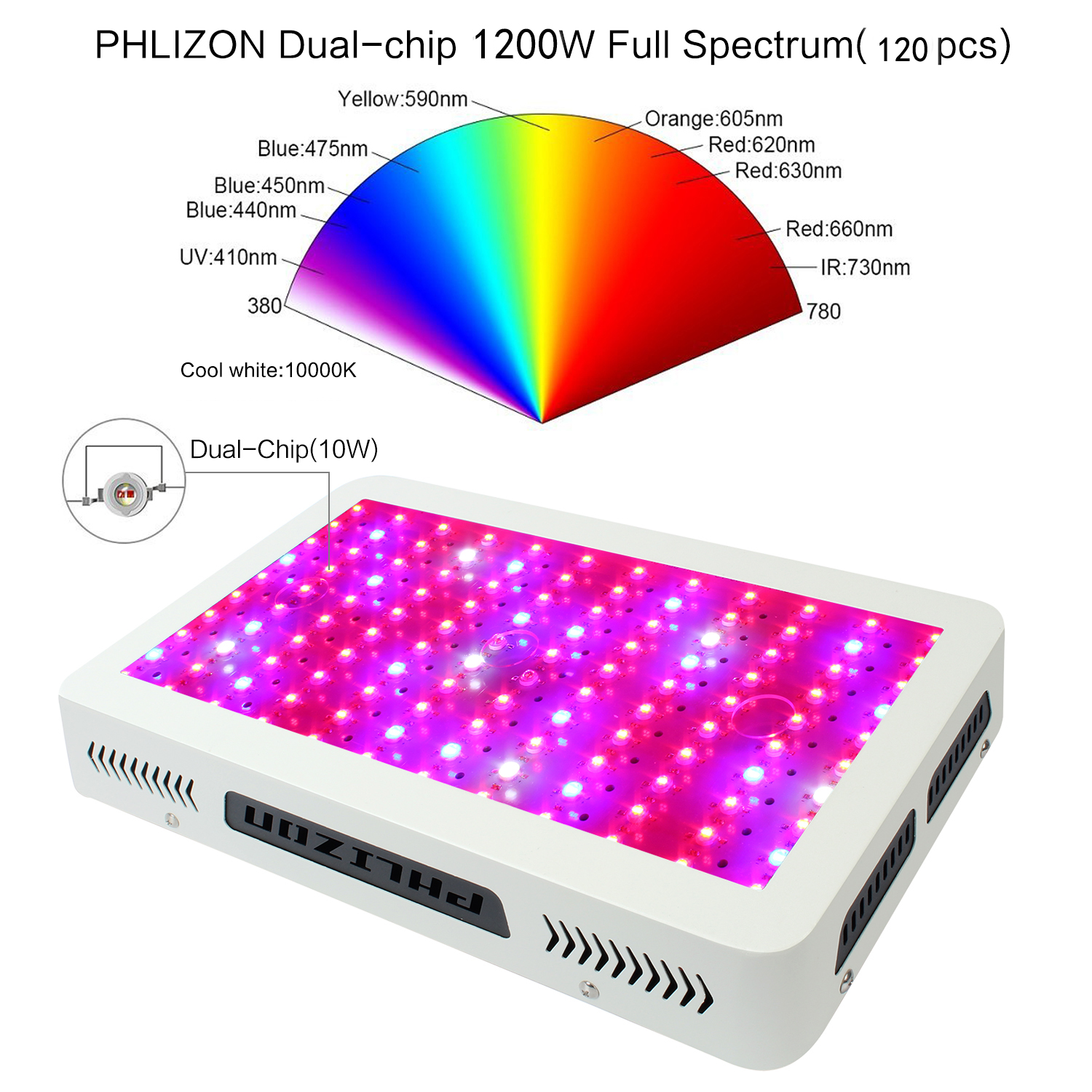
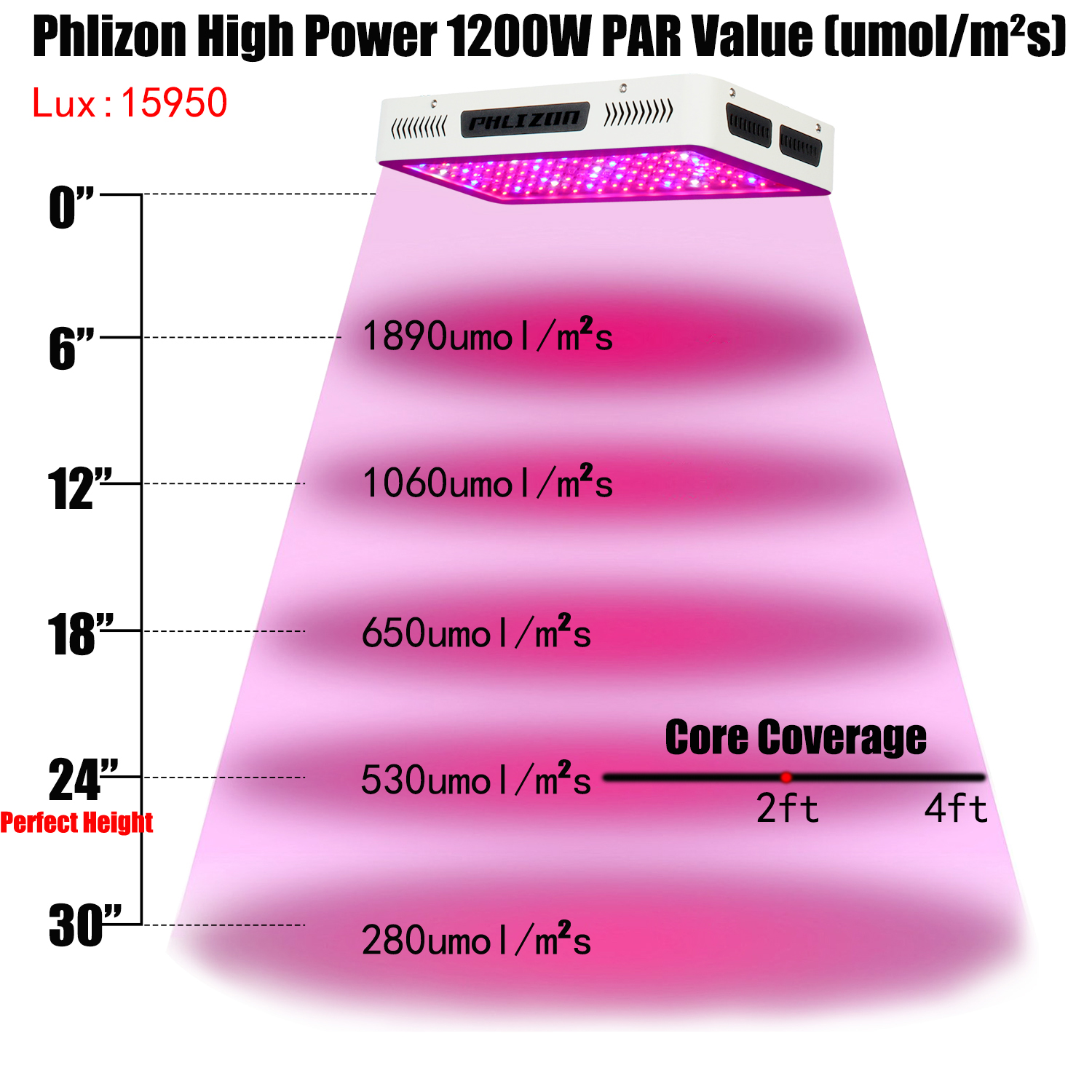
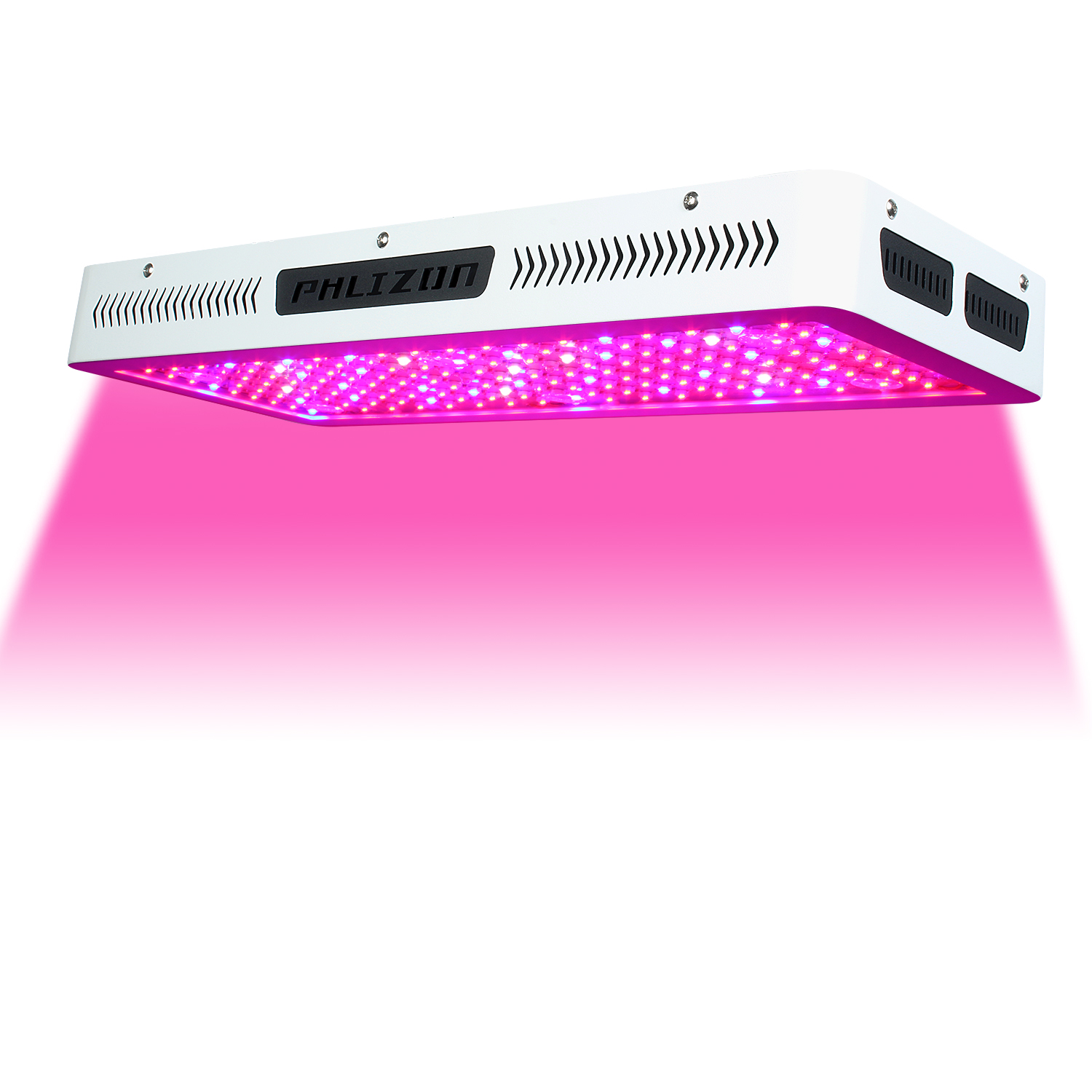
Product Images
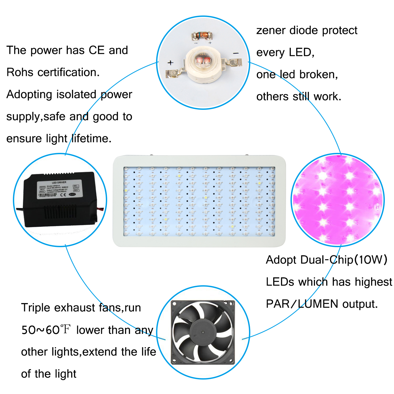
The Plug you can choose

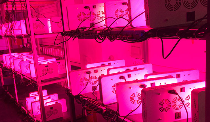
Ageing Test
Application
Our professional High Power Led Grow Light are suitable for all the indoor plants and good for seeding, growth,flowering and fruiting stages of plants, increasing the harvest and Saving energy.
Package


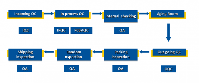
Quality Control Systems
Warnings:
1.lndoor use only.
2.To avoid being damaged,do not use water or drip irrigation while using.
3.Sunshine lighting time should be 12-18 hours.
4.While irradiating the plants,the height of led grow lamp is not less than 10 inches,low height will cause the destruction of plants.
5.Highly hang the lamp will weaken the energy and affect the growth cycle of the plants, so the lamp should not be hung too high.
6.While taking care of the plants, please spray the leaves and branches 2-3 times everyday,to ensure the the plants do not wrinkle a wither, and have no phenomenon of few fruit, and hard pericarp.
Trade Terms
Payment: T/T, L/C, Paypal, 30% deposits before production, 70% balance to be paid before deliverying(Western Union are welcome)
Sample will be delivered within 7 working days.
Discounts are offered based on order quanlityes.
MOQ:sample order are acceptable
Delivery ways:DHL,UPS,FedEx,TNT, door to door,by sea,by air,etc.
High Power Led Grow Light
New Design Grow Light,High Power Grow Light,High Power Grow Lamp,Led High Power Grow Light
Shenzhen Phlizon Technology Co.,Ltd. , http://www.philizon.com