Method for realizing multi-serial communication based on FPGA and SC16C554
0 Introduction With the rapid development of electronic technology, the performance-price ratio of general-purpose digital signal processors (DSPs) has been continuously improved, and data processing capabilities have been continuously strengthened. Its application fields are increasing day by day, and it is particularly widely used in real-time data acquisition and high-speed digital signal processing. . When DSP independently constitutes a processing unit, it often needs to exchange data with peripheral devices, and its communication ability is crucial. When developing an airborne synthetic aperture radar system, the signal processor as the core of the system must exchange data with the flight control system, stable platform, radar signal source and navigation system; how to achieve effective communication with other parts has become The key to system design. Serial communication is still one of the widely used methods because of its simplicity and reliability.
1 Serial port expansion scheme selection There are two common implementation schemes for multi-serial communication: one is software implementation, which uses software programming to simulate the serial port. This method has low cost, but the programming is complicated, the development cycle is long, and the reliability is low. The other is hardware implementation, which uses multiple serial port microcontrollers or special serial port expansion chips. Although this method has a higher cost, it is relatively simple to develop and has high reliability.
At present, the more general implementation scheme is to use a universal asynchronous communication chip to implement serial port expansion, and FPGA / CPLD to implement logic control between the DSP and the asynchronous serial port expansion chip, which is completely based on DSP to receive and send data. The disadvantage of this solution is that when the data volume is large and multiple serial ports work simultaneously, the DSP takes a long time, which affects the working efficiency of the DSP and causes data loss. Therefore, this paper proposes a new implementation method based on FPGA and universal asynchronous communication chip to achieve multi-serial communication design. On the basis of not making hardware changes, by establishing a buffer mechanism in the FPGA, the data of the serial port chip is received, and when a certain amount is reached, an interrupt reading data is sent to the DSP. This design can greatly reduce the occupation time of the DSP and improve the working efficiency of the DSP; at the same time, the response speed to the interrupt request of the serial port chip is improved, and the problem of data loss is solved.
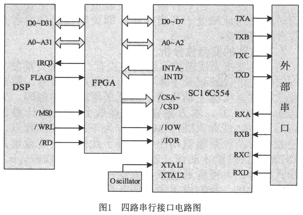
2 hardware circuit design This design uses the universal asynchronous communication chip SC16C554 to achieve serial port expansion. The main features of SC16C554 are:
1. There are four channels A, B, C and D to send and receive data independently;
2. The highest transmission rate can reach 5Mbit / s, with a programmable baud rate generator, which is convenient for flexible selection of data transmission and reception frequency;
3. With 16 bytes of transceiver FIFO, and there are four selectable interrupt trigger depths of 1, 4, 8, and 14 bytes;
4. The format of transmitted data (data length, parity bit, stop bit) can be set by programming;
5. With independent control of sending, receiving, line status and MODEM status interrupt;
6. Fully graded interrupt system control, comprehensive line status reporting function.
The basic principle diagram of multi-serial communication based on FPGA and SC16C554 is shown in Figure 1:
3 software design and implementation The actual baud rate required by the system is 9600, 38400, 115200 and 153600 respectively. When analyzing and calculating that data can be sent at different baud rates, the time interval between two consecutive data is shown in Table 1:
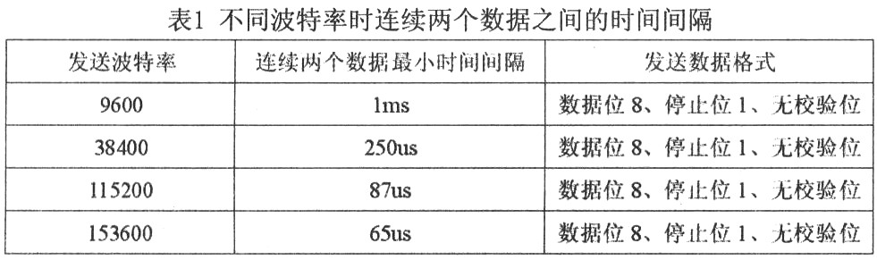
It can be seen from Table 1 that the minimum time interval between two consecutive interrupts generated by a single channel is 65μs; therefore, if data can be read from four channels at a time within 65μs, data will not occur even if four channels come at the same time. The phenomenon of data loss.
3.1 Data storage design That is to establish a cache mechanism within the FPGA. The design uses a dual-port RAM (DPRAM) inside the FPGA to store serial data, and the DSP obtains the received serial data by accessing the DPRAM.
DPRAM refers to a memory module but contains two independent ports. These two ports share the same block of address space. Both ports can write data to or read data from this block of space. The modes of reading and writing data of DPRAM include three modes of read-only, write-only, and read-write. Among them, the read-write mode includes three modes of write-first-read, read-first-write, and write-only-not-read. Mode.
We divide the address space of DPRAM into four parts, which are used to store four channels of data. When the FPGA receives data, we can determine which channel the data comes from based on the value of the set channel flag register CS [2: 0], store it in the corresponding address space, and add one to the corresponding address line of the channel. When the amount of data stored in the channel reaches the programmed trigger depth, the DSP interrupt register dspint is set low to send an interrupt to the DSP; at the same time, the channel flag is written to a pre-defined public storage space in the DPRAM. When the DSP receives the interrupt, it first accesses the common storage area to read the channel flag to determine which channel the interrupt was generated from; then it calls the corresponding receiving function to read the channel data from the DPRAM and store it in the specified address space Wait for processing.
3.2 Design of the serial port data read state machine A complete serial data read operation requires three read operations: read interrupt status register (ISR), read line status register (LSR), read receive save register (RHR). Because these three read operations have strict logic sequence and timing relationship, they are very suitable for description by state machine; therefore, this design uses finite state machine to read serial data. Figure 2 is a state transition diagram of reading channel A data.
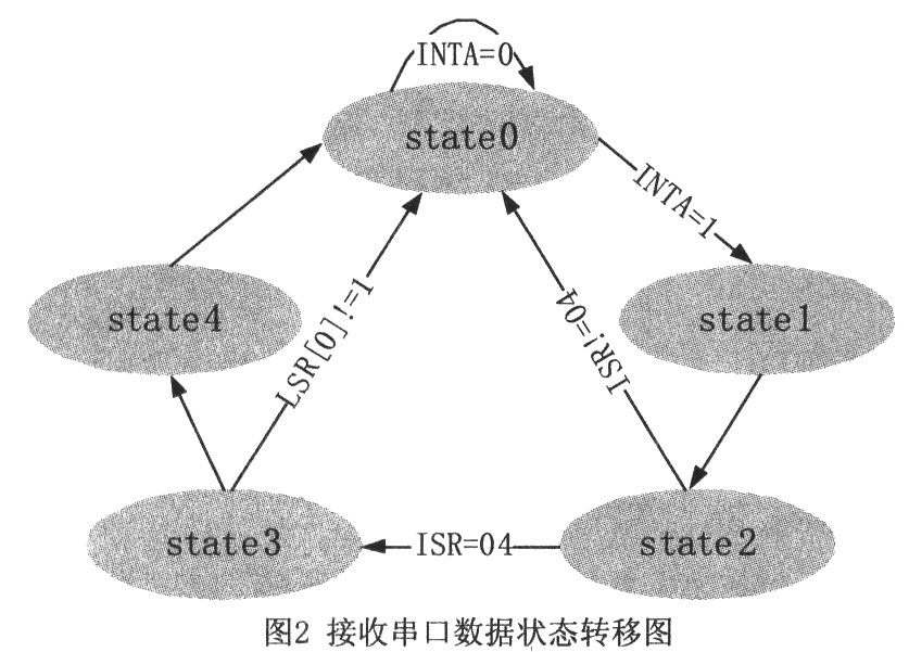
State0: Idle state, the state machine stays in the idle state when there is no data;
State 1: Assign the address of the IsR register to UART_A, and set the channel flag register CS [2: O] = 001 (indicating channel A);
State2: Read the ISR, determine the type of interrupt (04 is ready to receive data to interrupt), and assign the LSR register address to UART and A;
State3: Read LSR, judge whether there is data (LSR [0] = 1 means there is data in RHR), assign RHR register address to UART A;
State4: Read RHR, read serial data.
When working with multiple channels, it can be achieved by adding the state machine state. Four states are required to complete the reading operation of a channel. When the four channels work simultaneously, the state of the state machine needs to be increased to 17. Among them, Stare5 ~ State8 complete the operation on channel B; where State9 ~ State12 complete the operation on channel C; where State13 ~ State16 complete the operation on channel D.
3.3 Read timing design The general read timing diagram of SC16C554 is as follows:
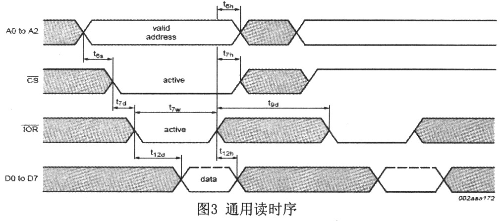
Among them t6s = 0ns t6h = 0ns t7h = 0ns t7d = 10ns t7w = 26nst9d = 20ns t12h = 15ns are the minimum value, t12d max = 26ns can be seen from Figure 3: the time required to read a serial port T = t6s + t7d + t7w + t9d so T is at least 56ns. This design uses the 60MHz clock to divide the 10MHz clock to complete a read operation within a 10MHz clock cycle (100ns). Synchronize a counter cscount [2: 0] with the 60 MHz clock, set CS low on the rising edge of the first 60 MHz clock (cs_count = 3'b000), and assign the corresponding address to UART A; The rising edge of the second 60MHz clock (when cs_cout = 3'b001) sets UART IOR low; the rising edge of the fourth 60MHz clock (when cs_count = 3'b011) sets CS and UART IOR high. In this way, the effective time of UART IOR is two clock cycles (33ns), and is delayed by one clock cycle (17ns) than CS, which fully meets the read timing requirements of Figure 3.
It can be seen from Figure 2 that it takes a total of 500ns from the idle state State0 to complete a serial data read. In this way, it takes 2 μs to complete the reading operation of four channels continuously during multi-channel operation, which is far less than the time interval of 65 μs generated by two consecutive interrupts of a single channel; this effectively solves the problem of other channels interrupted during the process of reading data when multi-channel operation The missing question. For example, when reading channel A data, channel B generates an interrupt request; then the state machine completes channel A data reading and returns to the idle state State0, detects that INTB is high, and the state machine enters the next state (State5) for channel B Data reception.
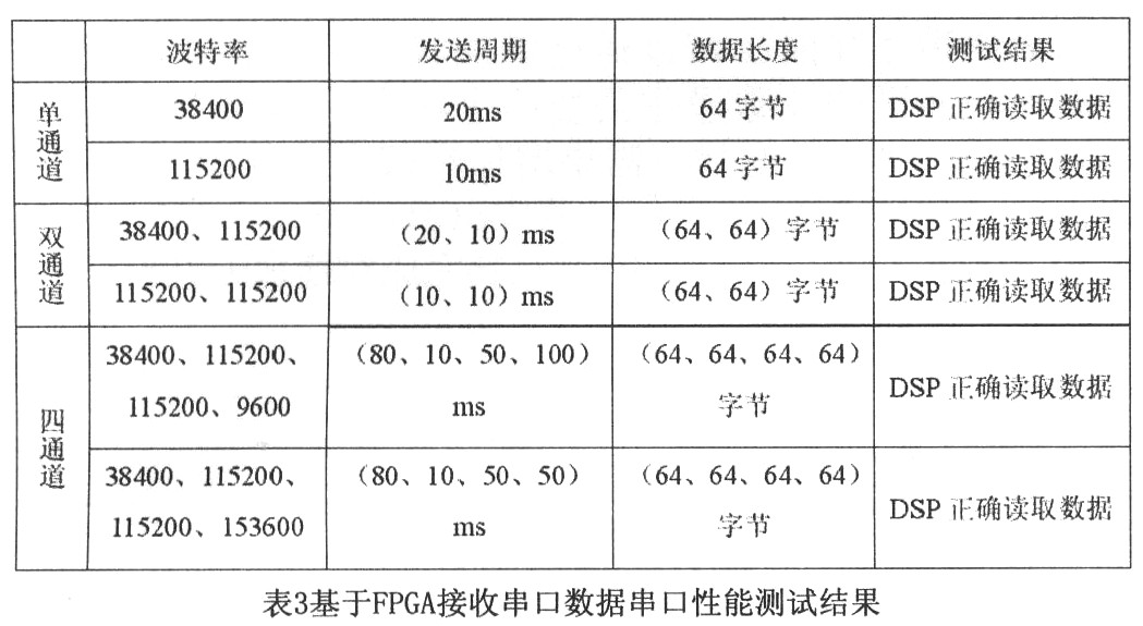
4 Test results and analysis We tested the two schemes separately, and the results are as follows: Table 2 is a communication performance test based entirely on DSP receiving and sending data; Table 3 is a communication performance test based on FPGA receiving serial data.
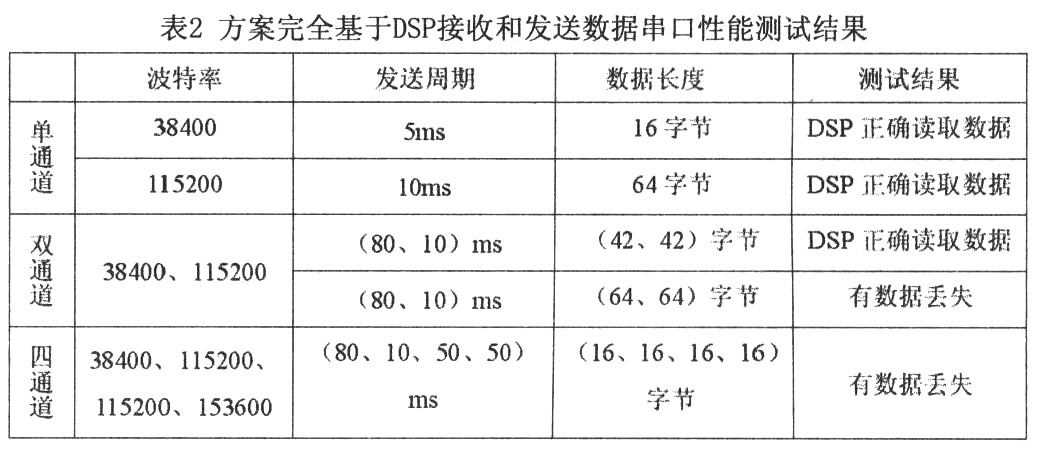
Baud rate transmission cycle data length test results Comparing the test results of the two schemes can draw the following conclusions:
1 When single channel works: The communication performance of the two schemes is the same.
2 When multiple channels work simultaneously: As can be seen from the test results in Table 2, each time the amount of data sent is too large, or the transmission cycle is small, data loss will be caused due to the processing speed of the DSP's interrupt request for the serial chip. It can be seen from the test results in Table 3 that when the four channels are working, the length of the transmitted data is 64 bytes, and the minimum transmission period of the channel is up to 10ms; if the length of the transmitted data is reduced, the transmission period of the channel can be smaller. The design performance is far better than the performance of receiving and sending data completely based on DSP before the scheme is improved; it can meet the needs of the actual work of the system.
5 Conclusion The design based on FPGA receiving data has two outstanding advantages: 1. It greatly improves the response speed to serial port interruption, avoids the multi-channel work, and completely loses the data when receiving and sending data based on DSP; 2. Fully programmable setting of DSP interrupt generation conditions, which solves the limitation of the original serial chip with only four trigger depths of 1, 4, 8, and 14 bytes. Programmable setting of trigger depth of any byte within the storage space greatly reduces DSP The number of interrupts improves the working efficiency of DSP. In addition, the program has strong portability. When the design needs to be modified, only a small amount of code needs to be modified, which effectively reduces the design cycle.
Modern Downlights,Mini Downlights,Smart Led Downlights,Led Ceiling Downlights
Changxing Fanya Lighting Co.,Ltd , https://www.fyledlights.com