Nand Flash memory is a kind of Flash memory, which provides a cheap and effective solution for the realization of solid-state large-capacity memory. NAND memory has the advantages of large capacity and fast rewriting speed, and is suitable for storage of a large amount of data, such as a digital camera, a memory card, and a compact U disk.
In 1989, Toshiba announced the Nand Flash architecture, which emphasizes lower cost per bit, higher performance, and can be easily upgraded via the interface like a disk. After more than a decade of development, NAND applications have become more widespread, but most engineers still don't know some difficulties about NAND applications: partitioning, ECC error correction, bad block management, and so on. Only engineers who truly understand NAND features can be applied in the application and will not be stumped by Nand Flash.
Partition
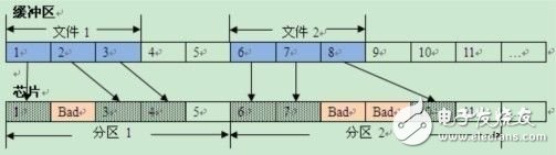
The essence of defining a partition is to define how data is written to NAND Flash, and data for different contents is written to the corresponding address. The average user will have multiple zones, such as boot, kernel, fs, user and other partitions.
Description of the partition: the address range of the partition (start block, end block), image size (Image Size).
Partition data storage: The image file is stored from the beginning block of the partition. If there are bad blocks in the partition, the bad block processing strategy will be used to replace the bad block until the image file ends. If the partition is not good enough to store the image file, then Burning failed.
The following figure is a schematic diagram of the image file partitioning of skipping bad blocks:
ECC (Error Correction) Algorithm
The ECC exists in the Spare Area of ​​each page of the NAND, which allows the external system to discover whether the data in the main area is incorrect. In most cases, the ECC algorithm can correct the bit errors, and NandFlash may also have bad blocks in use, so ECC is very necessary.
Different users may use different ECC algorithms. Generally, the ECC algorithm is provided by the processor vendor. If the ECC algorithm is not available in the programmer software, the user needs to provide the ECC algorithm source code.
If the user does not use the transfer file, but uses the method of reading the master to burn, and there is no dynamic data, the ECC algorithm can be ignored, because the spare area in the master has calculated the ECC and directly uses the spare area of ​​the master. Copy to other chips.
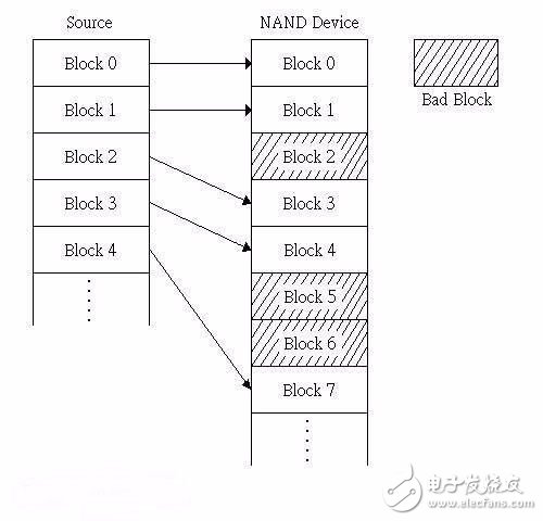
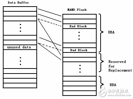
Bad block management
The bad block processing strategy defines how the algorithm should deal with when it encounters bad blocks. The basic bad block processing strategies are: skip bad blocks, replace tables (Reserve Block Area, RBA), etc. The bad block processing scheme is explained.
1, hard copy
Hard copy is actually dealing with bad blocks and processing nothing, no matter whether the good block or the bad block is directly programmed to burn the data in sequence, even if the check data is inconsistent, it is the simplest and direct processing method, but it can only be applied. A scheme in which data is not required to be managed;

2, skip the bad block
Skip bad blocks when you burn data, skip the bad block when you encounter bad blocks, and burn the data to the next good block. This ensures that all data can be written to the NAND memory space, but not Know which one the data burned to;
3, replacement table
In this method, some blocks are reserved in the NAND storage space as reserved blocks. When a bad block is encountered, one block is selected in the reserved reserved block to replace the bad block, and the data originally written to the bad block is written to the replacement block. in;
4, BBT (Bad block table)
The core of this method is to skip the bad block, but after skipping, you need to write a bad block table in the specified position of the NAND flash. The figure below is the structure diagram of BBT.

The points that need to be paid attention to in NAND applications are roughly as above. In actual use, there will be flexible application solutions. Engineers who need to be familiar with NAND characteristics and programmer principles can design suitable solutions. The P800Flash Extreme Speed ​​Programmer combines the features of ZLG Zhiyuan Electronics' third-generation Flash programmer, fully supports eMMC, NOR, NAND Flash programming, and provides a complete programming solution.
OPT Cutting Tools Co., Ltd. , https://www.optdiamondtoolss.com