MAX1239 OverviewThe MAX1239 is a 12-channel, 12-bit, low-power ADC featuring a 1.7MHz high-speed I²C-compaTIble serial interface. The MAX1239 supports both Fast / Standard mode (FS mode at 400kHz) and High-Speed ​​mode ( HS mode at 1.7MHz) with conversion rates up to 94.4ksps. HS mode is required to achieve conversion rates from 26ksps to 94.4ksps. External clock mode is required for conversion rates from 40ksps to 94.4ksps.
Hardware OverviewA simplified system block diagram is shown in Figure 1. The application circuit utilizes two evaluation (EV) kits: the MAX1238EVKIT with an installed MAX1239 (instead of a MAX1238), and a MAXQ2000-KIT. The MAX1239 was selected because of the digital -logic voltage range. The MAXQ2000 microcontroller's general-purpose input / output (GPIO) ports only accept up to + 3.3V; using level translators with high-speed I²C would have made the circuit overly complicated. The MAXQ2000 is not present on the MAX1238 EV kit board, so it was added to the system by connecting SCL, SDA, and GND on both boards. In addition, it is very important to apply + 3.3V (instead of + 5V) to VDD on the MAX1238 EV kit board. Order a free sample of the MAX1239EEE or MAX1239EEE + and solder it onto the MAX1238 EV kit. The modified MAX1238 EV kit schematic is shown in Figure 2.
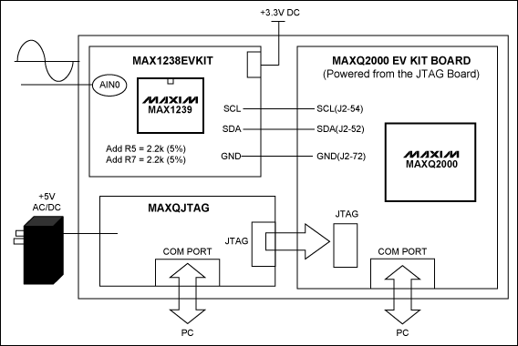
Figure 1. A simplified system block diagram.
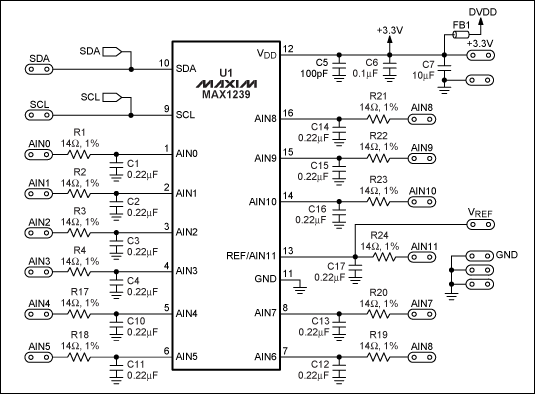
Figure 2. Modified MAX1238 EV kit schematic using a MAX1239.
The pinout of the MAX1239 allows easy isolation of the analog circuitry from the digital circuitry; the analog circuitry is grouped together on the left side of the board, and the digital circuitry is grouped together on the right side of the board. Keep this in mind when connecting the two boards together. Connect J2-52 (SDA) on the MAXQ2000 EV kit board to the SDA pad on the MAX1238 EV kit. Similarly, connect J2-54 (SCL) to the SCL pad. The grounds of both boards must be connected together. In addition, R5 and R7 both have to be populated with 2.2kΩ 5% resistors. The MAX1238 EV kit already has 47kΩ I²C pullup resistors and the MAXQ2000 EV kit has 10kΩ I²C pullup resistors. Adding R5 and R7 will provide approximately 1.6kΩ of pullup resistance on the I²C bus.
The MAXQ2000 EV kit contains a complete set of hardware, software, sample code, and documentation needed to start designing with the MAXQ2000. Schematics for the MAXQ2000 EV kit are available in the data sheet.
Firmware OverviewThe example firmware was developed using the free MAX-IDE Version 1.0. Download the latest version of the MAX-IDE.
The main source file is hsi2c.asm, and it was written in assembly to optimize the timing of the HS-mode I²C interface. The source code does the following things: a) Initializes the MAXQ2000's UART for 8-N-1 at 115.2kbps
b) Initializes the MAX1239 CONF BYTE for single-ended channel AIN0
c) Initializes the MAX1239 SETUP BYTE for the internal reference, external clock, and unipolar operation
d) Initializes the MAX1239 for I²C HS mode
e) Reads back 12-bit samples from the MAX1239 in I²C HS mode
f) Transmits the 12-bit samples over the serial port The example assembly program collects samples from the MAX1239 by bit-banging a HS-mode I²C interface on the MAXQ2000's GPIO ports. The MAXQ2000's 16MHz system clock allows the bit-banged HS-mode I²C interface to run up to 1.7MHz.
The hsi2c.asm file defaults to the slave address of the MAX1239EEE or MAX1239EEE +. The firmware must be customized for each different part in the family. For example, follow the two steps below when using the MAX1239KEEE, MAX1239KEEE +, MAX1239LEEE, MAX1239LEEE +, MAX1239MEEE, or MAX1239MEEE +: Edit the I2C_ADDR define statements to reflect the I²C address of the part used. These variables are required to be the compliment of the actual address. For example, an address of 0111 111 (r / w) needs to be encoded as: I2C_ADDR7 equ 1
I2C_ADDR6 equ 0
I2C_ADDR5 equ 0
I2C_ADDR4 equ 0
I2C_ADDR3 equ 0
I2C_ADDR2 equ 0
I2C_ADDR1 equ 0 The source code expects a 16MHz system clock to be used (MAXQ2000 crystal). The following figures illustrate the FS-mode (Figure 3) and HS-mode (Figure 4) I²C frames implemented in this application note.
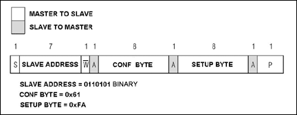
Figure 3. FS-mode two-byte write operation.
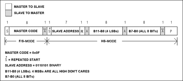
Figure 4. HS-mode receive operation.
Figures 5 through Figure 16 are scope shots of the FS-mode (Figure 3) and HS-mode (Figure 4) I²C frames implemented in this application note. Channel 1 is SCL and Channel 2 is SDA on all scope shots.
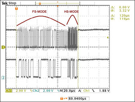
Figure 5. A complete frame of all the I²C communication (FS-mode and HS-mode operations).
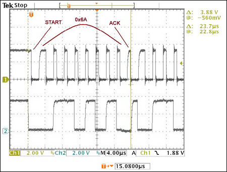
Figure 6. FS-mode operation, Byte1 (start + Addr = 0x6A + ACK).
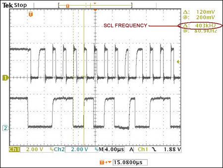
Figure 7. The SCL clock frequency in FS mode is approximately 400kHz.
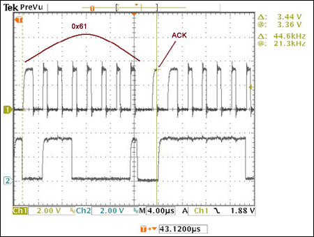
Figure 8. FS-mode operation, Byte2 (conf byte = 0x61 + ACK).
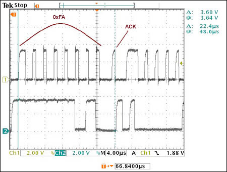
Figure 9. FS-mode operation, Byte3 (setup byte = 0xFA + ACK).
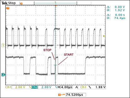
Figure 10. FS-mode operation, stop and start of next operation (stop and start).
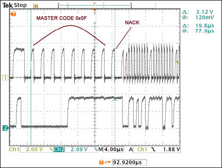
Figure 11. FS-mode operation, Byte4 (master code = 0x0F + NACK).
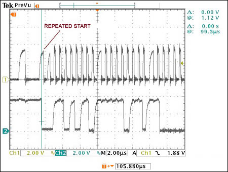
Figure 12. HS-mode operation, repeated start.
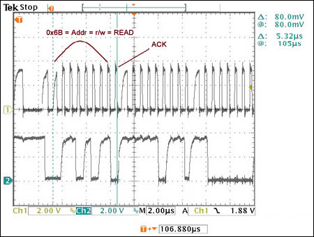
Figure 13. HS-mode operation, Byte5 (Addr = 0x6B + ACK).
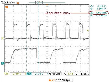
Figure 14. The SCL clock frequency in HS mode is approximately 1.7MHz.
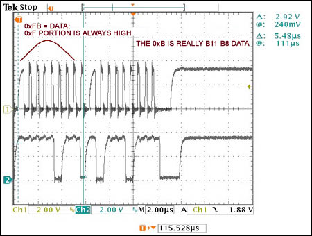
Figure 15. HS-mode operation, Byte6 (data = 0xFB + ACK).
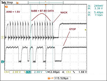
Figure 16. HS-mode operation, Byte7 (data = 0xBB + NACK + FS-Stop).
The specification for high-speed I²C has existed since January 2000. Nonetheless, few, if any microcontrollers are available today with an internal high-speed I²C peripheral. This is an unfortunate situation since several devices, such as ADCs, DACs, CODECs, and even power supplies, are being designed to support the high-speed I²C interface. This application note provides a much-needed working, high-speed I²C example.
Download: Source Code
We are the professional manufacturer of Li-ion polymer Cell Phone Battery with over 7 years experience major involved in Iphone Battery ,Huawei Battery, Samsung Battery ,Iphone High Capacity Battery,Cell Phone Accessories,Wireless Car Charger and etc.
With full capacity polymer lithium battery and 100% pure cobalt cell which life span
Up to 800 cycles, our cellphone battery adopts the original IC protection board to be more durable, stable and safe.
The Cell Phone Battery uses the imported high quality IC chips with original seal,from the storage of the cell to the output, it breaks through the shortage of the previous chip conversion rate of 99% and comprehensively upgrades the conversion rate to 99.9%.
Our Mobile Phone Battery is designed of double fuse to prevent short circuit,automatic short circuit recovering with the memory metal fuse.
Five security makes the cellphone more competitive:1)Strong power storage 2)Quick charge 3)Durable upgrade 4)safe using 5)High efficiency.
The Cell Phone Battery replacement adopts fully automated high-tech, the daily production of batteries reaches 12,000 pieces, each battery has passed dozens of strict tests, the defect rate is less than 3%.
The Cell Phone Battery has multiple protection functions, which can effectively protect the battery, and will automatically disconnect when it is fully charged.Multiple protection functions include temperature protection, circuit protection, Reste protection, input voltage protection, hardware over-current protection, output over-current protection, input anti-reverse protection, battery over-pressure protection.
Cell Phone Battery
Cell Phone Battery,Phone Battery,Mobile Phone Battery,Mobile Battery
Shenzhen Hequanqingnuo Electronic Technology Co., Ltd. , https://www.hqqnbattery.com