The most challenging aspect of a switching power supply is the loop parameters. It is very difficult to determine them accurately. Usually, the system's stability is not stable.
During the early stages of the power supply design project, attention should be given to various detailed parameters.
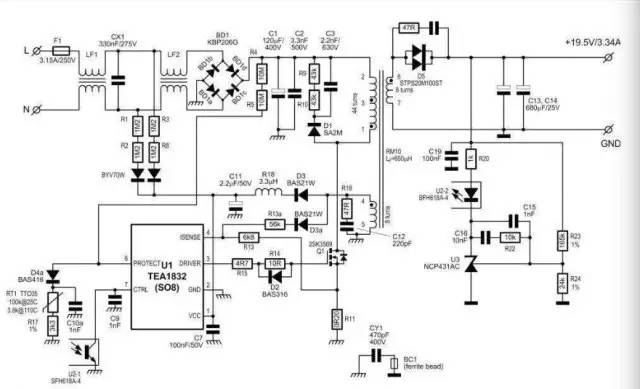
By learning from the TEA1832 schematic by NXP, we analyzed the circuit design and optimization of the parameters and achieved certification for mass production. We tried to select components from the company's warehouse and use larger components to facilitate subsequent cost reduction.
Chip resistors are available in 5% tolerance for 0603 and 0805 packages, and 1% for other sizes. The higher the capacitance of the chip capacitor, the more expensive it is, so design considerations must be made accordingly.
1. Input fuse selection requires consideration of the I²T parameter. Fuses are classified as fast or slow blow, with specific current and voltage values. Fuse certification must be complete. The safety distance before the fuse should be at least 2.5mm, preferably 3mm or more. When considering lightning strikes, ensure there is a margin for the fuse I²T to avoid failure.
2. A varistor can be added to this figure, typically using 14D471 or 561. Larger diameters provide better surge current resistance. Enhanced versions like 10S471 or 14S471 may also be used. Generally, 14D471 can withstand 1kV or 2kV lightning strikes. If necessary, a heat shrinkable sleeve can be placed around the varistor.
3. An NTC thermistor can be added to this figure. Some customers limit the inrush current during startup to no more than 60A or 30A. Additionally, an NTC can help reduce the voltage during lightning strikes, reducing stress on the MOSFET. Pay attention to the NTC's voltage, current, and temperature ratings when selecting.
4. Common-mode inductors are crucial for filtering conduction and radiation. They often use high-conductivity materials such as 5K, 7K, 0K, 12K, 15K. Winding methods include slot winding, wire winding, and butterfly winding. There are UU-type and ET-type inductors with four slots. If possible, share the best parts from the old model to reduce costs, finalized after conducting and radiation tests.
5. X-capacitor selection should be combined with common-mode inductor testing for conduction and radiation. Generally, the greater the power, the larger the X-capacitance.
6. If there is a discharge time requirement for input L and N during authentication, two strings of resistors should be connected to discharge the capacitor under the X-capacitor.
7. The choice of bridge stack generally involves considering the surge current, voltage, and heat dissipation of the bridge stack to prevent failure during lightning strikes.
8. VCC starting resistor: pay attention to the power consumption of the starting resistor, mainly the withstand voltage value. Typically, 1206 has a withstand voltage of 120V, while 0805 has 150V, leaving more room for better performance.
9. Input filter electrolytic capacitors usually consider cost. The output retention time is 10ms, and the minimum capacity of the electrolytic capacitor is designed at 80% of its capacity. Different manufacturers and design experiences vary slightly, so attention should be paid to ordinary electrolytic capacitors and lightning-resistant electrolytic capacitors. Ripple current of the electrolytic capacitor relates to its lifespan, depending on the brand and series.
10. A small ceramic capacitor is connected in parallel with the input electrolytic capacitor. This usually does not show its usefulness but can have an effect during conducted immunity tests.
11. RCD absorption part: the value of R corresponds to the peak voltage on the MOSFET. If a chip resistor is used, attention should be paid to voltage derating and power consumption. C generally takes 102/103 1KV high-voltage ceramic tiles, and may be changed to film capacitors when rectifying radiation. D generally uses FR107, FR207, and when radiation is rectified, it may be replaced with 1N4007 or other slow tubes, or magnetic beads (K5A, K5C, etc.) can be placed on D. For low power, RC can be replaced by TVS tube, such as P6KE160.
12. MOSFET selection: consider the surge current, voltage, and heat dissipation of the MOSFET to prevent failure during lightning strikes. At high temperatures, current derating is needed, and at low temperatures, voltage derating is required. Generally, 600V 2-12A is sufficient for flyback within 100W, and the selection should be weighed according to cost. When many methods fail during radiation rectification, it is often due to a MOSFET issue.
13. MOSFET drive resistance is generally 10R + 20R. The resistance value corresponds to the switching speed, efficiency, and temperature rise. This parameter needs to be adjusted when rectifying radiation.
14. A 10K-100K resistor should be added between the GATE and SOURCE terminals of the MOSFET to discharge.
15. There is an Isense resistor between the SOURCE and GND of the MOSFET. The power should be as large as possible. Try to use a wound non-inductive resistor. If the power is small, or if there is a short circuit in the sense resistor, it may result in a "bomber" phenomenon.
16. Isense resistance to IC's Isense increases by 1 RC, the value is 1K, 331, which may play a role in debugging. If this TEA1832 circuit is used as a reference, add a C parallel to GND.
17. Different IC peripheral pin reference design manual, according to their own experience, put the filter capacitor at the IC pin.
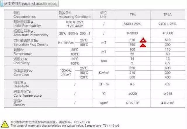
18. Transformer design: discuss the flyback transformer design forum, not much to say. Still consider the cost, try not to add a shield inside the transformer, at most, add a cross shield outside the transformer. The transformer must check the delta B value to prevent core saturation at high temperatures. Delta B = L * Ipk / (N * Ae), L (uH), Ipk (A), N is the primary number of turns (T), Ae (mm²). Refer to TDG's core characteristics (100°C) saturation magnetic flux density 390mT, remanence magnetic 55mT, so the ΔB value is generally within 330mT. Abnormal situations do not saturate, generally less than 300mT. I used to do the flyback transformer values are less than 0.3, learn zhangyiping experience (so the general flux density chooses 1500 Gauss, the transformer can be smaller, the transformer should be smaller, the frequency is lower. The lower one can be bigger.)
The VCC auxiliary winding of the transformer should be wound with more than 2 wires as much as possible. In the previous large batch, there were several auxiliary windings with insufficient light load voltage or VCC overvoltage at heavy load. 2 and above VCC auxiliary winding lines can be coupled as much as possible to solve the problem of large voltage differences.
Note: If you are interested in verifying this formula, you can input at the lowest voltage and increase the output load. When you see the saturation waveform of the transformer, the calculation result should be about 500mT when saturated (the saturation magnetic flux density is 510mT at 25°C).
Learn from the basic characteristics of the magnetic core of TDG.
19. When the output diode efficiency is high, an ultra-low dropout Schottky diode can be used. When the cost is high, an ultrafast recovery diode can be used.
20. The RC in parallel with the output diode is used to suppress voltage spikes and also suppress radiation.
21. Optocoupler and 431: the optocoupler diode can increase a resistance of about 1K-3K, the resistance of Vout series to the optocoupler is generally between 100 ohm-1K. C and RC on 431 are used to adjust loop stability, dynamic response, and so on.
22. Vout detection resistance needs to have a current of about 1mA. The current is too small, the output error is large; the current is too large, affecting standby power consumption.
23. Output capacitor selection: the ripple current of the output capacitor is approximately equal to the output current. When the capacitor is selected, the ripple current is amplified by 1.2 times or more.
24. A small inductance can be added between the two output capacitors to help suppress the radiation interference. With a small inductance, the ripple current of the first output capacitor will be much larger than the ripple current of the second output capacitor. Therefore, in many circuits, the first capacitor has a large capacity, and the second capacitor has a small capacity.
25. The output Vout terminal can add a common mode inductor in parallel with the 104 capacitor to help conduct and radiate, and also reduce the peak-to-peak ripple.
26. If there is a need for constant current, professional chips such as AP4310 or TSM103 can be used, or 431 + 358 is acceptable. Pay attention to the VCC voltage range, loop adjustment is similar.
27. If there are multiple output load conditions, the main feedback circuit of the power supply must have a fixed output or a dummy load. Otherwise, the output voltage of other channels may be unstable due to coupling, burst mode, and other problems.
28. There is a Y capacitor between the primary and secondary ground. The general capacity is less than or equal to 222, and the leakage current is less than 0.25mA. Different product certifications have requirements for leakage current.
Counting down so much, the electronic components can basically be finalized, and the entire initial BOM can be reviewed and referenced. Components in the BOM can be placed in several brands to facilitate the cost of the core. If the customer has special requirements, you can add functional circuit implementation in the circuit. If it is not possible to find a new IC to complete, IC power changes have little effect on peripheral devices at equal power and frequency. If the customer's temperature range is relatively high, the corresponding component options need to refer to the component temperature and derating.
2. The details of the power PCB design stage should pay attention to:
1. The SCH network corresponding to the PCB should correspond to the subsequent update, which will not take much time.
2. PCB component packaging, the standard library needs to be changed according to the actual situation, the patch component pad is enlarged; the aperture of the plug component is 0.3mm larger than the component pin, and the pad diameter is larger than the hole 0.8mm or more. The disk is more convenient for soldering, and the components are too easy to solder on the wave soldering. It is not easy for the PCB manufacturer to make holes. There are still a lot of details to know more about the production is a great credit.
3. The requirements of safety regulations on the PCB, the safety input of the fuse to the output distance of more than 3mm, the fuse belt model needs to be printed on the PCB. PCB boards also have different safety requirements, and the corresponding certifications and supplier communication can meet the requirements. The corresponding certification number must be printed on the PCB. The distance from primary to secondary is 8mm or more, Y capacitor is required to choose Y1 or Y2, the span is also required to be 8mm or more, the primary and secondary of the transformer, and the three-layer insulated wire flying line with the retaining wall or secondary is used for creepage distance.
4. The distance between the L and N lines in the front of the bridge is more than 2.5mm, and the high voltage + after the bridge is piled up, and the distance is more than 2.5mm. The trace is the first for the high current loop, and the smaller the area, the better. The signal line is away from the large current trace to avoid interference. The filter capacitor of the IC signal detection part is close to the IC, the signal ground is separated from the power ground, the star ground is grounded, or the single point is grounded, and finally summarized to the "- " pin of the large capacitor. Avoid signal interference during debugging or immunity.
5. IC direction, the direction of the chip components, as far as possible into the entire row of columns, to facilitate the wave soldering on the tin, improve production line efficiency, avoid shadow effects, even tin, solder joints and other issues.
6. The components of the AI need to be placed according to the corresponding rules, before looking at a Japanese PCB, the pad is made into a drop shape, the AI component's pin just on the drop-shaped pad, beautiful.
7. The trace on the PCB has a greater impact on radiation, you can refer to the relevant books. There is also a case where the PCB is wired as a single panel. After the completion of the PCB, it is effective to suppress the conduction and radiation by applying a large piece of copper to the top layer.
8. When wiring, you need to consider lightning strikes, ESD or other disturbing current paths, will affect the IC.
3. The details of the power supply debugging phase should pay attention to:
1. The multimeter first tests the diode on the main current loop, the MOSFET, whether there is a short circuit, whether it is installed or not, whether the transformer's sense and leakage inductance are tested, and whether the transformer has the same name or not.
2. Start to power on, my habit is to first on the low voltage of 100V, PWM has no output. Use the oscilloscope to see VCC, PWM pin, VCC rises to the startup voltage, and PWM has no output. Check if the protection function of each pin is triggered or the parameters are incorrect. Can't find the problem, check the power-on timing diagram of the IC, or the IC boot condition in the IC's datasheet. When using the oscilloscope, please pay attention to the ground wire of the 3-pin plug to be unplugged. If it is not unplugged, it is better to use the isolation probe to hang the waveform. When using two or more probes, the COM terminals of the two probes are connected to the same point to avoid affecting the circuit or burning the wrong position.
3. IC startup problem is solved, PWM has output, found that the transformer screams at startup. The current waveform of the MOSFET is connected, or whether the waveform of the Isense foot is a triangular wave, it may be a saturated waveform, and may be a square wave. It is necessary to recalculate ΔB. In other cases, the VCC winding and the main winding are wound around the wrong position. There are also cases where the output is short-circuited, and there is a problem with the RCD absorbing portion, and even the TVS is broken.
4. The output is there, but the output voltage is wrong, or high, or low. This needs to be judged from the primary to the secondary or the secondary. Hanging output diode voltage and current waveform, whether it is a normal flyback waveform, the waveform is wrong, it is estimated that the same name end is reversed. Check if the optocoupler is damaged, the optocoupler is normal, and replace the position of 431 with the +1K resistor of the Zener tube to judge the output feedback 431 part, or the protection action of constant current or overload protection. Frequently asked questions, the optocoupler pin is wrong, resulting in feedback that cannot be reached. The 431 package is wrong. Generally, there are two kinds of 431 packages, and the pins are mirrored. Problems with the same name can cause the output voltage to be incorrect.
5. The output voltage is normal, but not accurate 12V or 24V, this time generally uses two resistors in parallel to adjust to the precise voltage. The sampling resistor must be 1% or 0.5%.
6. The output can be loaded, with a full load transformer has a sound, the output voltage ripple is large. Hang the PWM waveform, whether there are large or small waves or dozens of cycles, stop for dozens of cycles, this situation adjusts the loop. C and RC on the 431, many of the ICs now have integrated compensation, and the loops are better adjusted. The loop adjustment has no effect. It can be calculated that the inductance is too large or too small, and the Isense resistance can be re-calculated. Whether the IC has considered the Isense resistance voltage is small, the IC works in the brut mode. The Isense resistance value test can be changed.
7. High and low voltage can be fully loaded, the waveform is normal. Test the power efficiency. When inputting 90V and 264V, the efficiency should be consistent (change the duty cycle, turn ratio) to facilitate the subsequent safety test temperature rise. Power efficiency generally refers to the efficiency of the old model, or check the standard reference in the energy efficiency rating.
8. Output ripple test, generally require 47uF+104, or 10uF+104 capacitor test. The capacitance of this electrolytic capacitor affects the ripple voltage, and the high frequency and low resistance of the capacitor (different brands and series) also affect the ripple voltage. When the oscilloscope is testing the ripple, the spring test probe is used on the probe to avoid interference peaks. In the case that the output ripple is uncertain, you can change the capacity, change the series of capacitors, and even consider the use of solid capacitors.
9. Output overcurrent protection, customer requirements for high precision, in the secondary discharge current protection circuit, the requirements of low precision, general primary overcurrent protection, most ICs have integrated overcurrent or overpower protection. Overcurrent protection typically amplifies 1.1-1.5 times the output current. At the maximum output current, the stress of the component needs to be tested with a margin. Current protection, such as increasing the feedback loop, can be made into a constant current mode, and the no feedback loop is generally a snoring protection mode. To do over-current protection, it is also necessary to test the test of full-load + electrolytic capacitors. The requirements sometimes requested by the client do not give a question of whether it is a capacitive load, and how much capacity can be taken up after testing.
10. Output over-voltage protection, customers with high stability requirements will require two optocouplers, one for normal operation and one for over-voltage protection. No requirement, increase the overvoltage protection circuit at the auxiliary winding of VCC, or there is integrated overvoltage protection in the IC, and there are few peripheral devices.
11, over-temperature protection generally depends on the specific circumstances added, safety standards are required for high-temperature testing, can meet the safety requirements of the temperature can be, unless the environment is complex or abnormal, you need to increase the over-temperature protection circuit.
12, start-up time, the general requirements for 2S, or start within 3S, are better to do, standby power to achieve a very low power solution, the general IC is considered. no problem.
13. Rise time and overshoot, this is achieved by adjusting the soft start and loop response.
14. Load regulation and linear regulation are achieved by adjusting the loop response.
15. Hold the time and change the input capacitance.
16, output short circuit protection, now IC short circuit protection is getting better, generally short circuit, IC VCC auxiliary winding voltage is low, IC is powered by starting resistor, after IC startup, Isense pin detection over current will do short circuit protection, stop PWM Output. Generally, the short-circuit power is maximum at 264V input, and the short-circuit power is safer to control within 2W. When short-circuiting, you need to test the current and voltage of the MOSFET, and check whether the short-circuit is beyond the design range by looking at the SOA diagram (safe working area) of the MOSFET.
17. After the no-load starts, the output voltage jumps. It is possible that the VCC auxiliary winding induced voltage is low at light load, increasing the number of VCC winding turns, and possibly the output feedback loop is unstable, and the loop parameters need to be updated.
18. The voltage will not come up when the loader starts or the load is heavy. When the load is heavy, the VCC auxiliary winding voltage is high, and it is necessary to check whether overvoltage or overcurrent protection action.
In addition, the transformer is designed according to the normal output load design, resulting in saturation of the transformer before heavy load or overcurrent protection.
19, the stress of the components should be tested, full load, overload, abnormal test component stress should have a margin, the size of the balance depends on the company's regulations and cost considerations. Performance testing and debugging are basically completed. When you debug, think of yourself as the person who designed this IC, you can understand the working condition of the IC and solve the problem quickly.
4, EMC and other attention before the test details
1, temperature rise test, 45 ° C oven environment, input 90,264 transformer core, line package does not exceed 110 ° C, PCB within 130 ° C. The specific values of other components refer to the following safety regulations. The most difficult temperature is generally the transformer.
2, insulation withstand voltage test DC500V, resistance value is greater than 100MΩ, primary and secondary AC3000V time 60S, less than 10mA, production line mass production can play AC3600V, 6S. It is recommended to use DC voltage DC4242 to withstand voltage. The withstand voltage is set to 10 mA. During the test, the test instrument alarms, check the primary and secondary distances, the primary to the outer casing, and the secondary to outer casing distance. It is better to pull the test room onto the curtains, and quickly find the spark at the discharge position.
3. The impedance to ground is generally less than 0.1Ω, and the test condition current is 40A.
4, ESD generally requires contact with 4K, air 8K, there is a resistance and capacitance model problem. Generally, the level will be increased, hitting the highest contact 8K, air 15K. When playing ESD, if there is a discharge needle under the common mode inductor, the discharge pin will discharge. The ESD of the power supply also ignites between the heat sink and the different components, which is generally a distance problem and a layout problem of the PCB. When playing ESD to 15K, the power supply is broken and you know how much voltage your power supply can resist. When you do safety certification, you have a bottom. If the customer has a higher voltage, they know how to deal with it. Refer to EN61000-4-2.
5, EFT this has not had a problem 2KV. Refer to EN61000-4-4.
6, lightning strike, differential mode 1K, common mode 2K, using pressure sensitive 14D471, there is input large electrolysis, there is no big problem with the basic PASS. In the case of lightning strikes, the low power 5W, 10W hangs, using electrolytic capacitors that can resist lightning strikes. The unipolar PFC is used to fly back and hang the MOSFET. After the input bridge stack, a diode is connected in series with the electrolytic capacitor, and the capacitor absorbs energy. When the LED power supply is 2K and 4K, the 4KV is in the form of a varistor + GDT. Refer to EN61000-4-5.
EFT, ESD, SURGE have A, B, C grades. Generally, the A grade: interference has no effect on the power supply.
7, low temperature start. Generally cheap power supply, temperature range is 0-45 ° C, expensive, industrial, or LED what is required -40 ° C -60 ° C, or even 85 ° C. At -40 °C, the input NTC is increased by N times, the input electrolytic capacitor is obviously not enough, the ESR is very large, and the PFC is also a little dangerous if the 500V MOSFET is used (the MOSFET withstand voltage becomes low at low temperature). The output voltage jumps when the 90V input is encountered before, or the LED flashes several times to be normal. Increase input capacitor capacity, change NTC, increase VCC capacitor, soft start time is longer, primary current limit (input capacity is not enough, resulting in low voltage, large current, trigger protection) from 1.2 times to 1.5 times. The VCC winding of the IC increases the 2T auxiliary voltage boost; if the protection circuit is too limited, the low temperature is triggered (for example, the PFC overvoltage is easily triggered).
5, conduction rectification attention to details
The basic performance and safety basic problems are solved, leaving a conduction and radiation problem. At this time, you can talk to the customer about the follow-up price and optimize the line. Confirm the safety problem with the safety engineer, and confirm with the production line engineer whether the components on the PCB need to be changed in position, and whether the production line is convenient to operate. Or there is the problem of playing AI, reflow soldering wave soldering, and timely adjustment of components.
1, conduction and radiation test everyone sees more, the forum also talks about more, in fact, this is a money-saving thing. If you save more money, it will be natural, and the rectification will be faster. There are only a few places that can be changed. 1, this can not be seen inside, especially important is the PCB, there are powerful can find the line on the PCB, cut, change the way to get rid of 3 dB, the balance will be.
2, generally see the notebook power adapter, the computer part has a very ugly flaw, this is an EMI filter, from the outlet part of the adapter to the laptop so long distance, can be seen as an antenna, increase A filter can filter out the loss. Therefore, the output of the general switching power supply has a filter inductor, and the effect is the same.
3, input filter inductor, power is small, UU type is very easy to use, the power is basically used ring type and ET type. If the company has a conducting laboratory or a conducting instrument, it can be tossed if there is an idea. If you want to go to a third-party laboratory, it will be more painful. The filter inductor is better with high-conductivity 10K material, and the effect on the conducted radiation suppression is good. If the conduction is poor, it can be changed to 12K, 15K. If the radiation is poor, the material can be changed to 5K or 7K.
4, input X capacitor, can use small to use small, mainly occupying the place. This should be adjusted with the filter inductor.
5, Y capacitor, the first secondary does not have a Y capacitor, or the Y capacitor is very small, generally from 150K-30M are floating, or fly out of the limit, and installed a 471-222 is almost. The connection of the Y capacitor directly affects the test data of conduction and radiation, generally the primary ground connection to the secondary ground, the primary high voltage, the secondary ground, or the two primary capacitors of the Y capacitor and the primary ground. No one can say before the adjustment. The magnetic beads on the Y capacitor have an effect on 10MHz or more, but not all. Everyone has different methods and methods for debugging conducted radiation. The models are different and the problems are different, so maybe my method is only suitable for my own use. Most of the non-Y solutions are made by changing the transformer, and the power is not good.
6, MOSFET absorption, DS can directly connect to a maximum of 221, or the temperature is too high, generally 47pF, 100pF. RCD absorption, can be a string of 10-47Ω resistor absorption peak on C. It is also possible to string a 10-100 Ω resistor on D, and the MOSFET drive resistance can be changed to within 100 Ω.
7, the absorption of the output diode, generally using RC absorption is sufficient.
8, transformers, transformers have copper foil shielding and wire shielding, copper foil shielding has good conduction effect, wire shielding has good radiation effect. As for the initial package, at the beginning of the package, there are some other winding methods to better control the radiation.
9. For the PFC to do the flyback power supply, the input part also needs to increase the differential mode inductance. Generally, it is made of a rod-shaped inductor or a yellow-white ring of an iron powder core.
10. When rectifying the conduction, try to reduce the amount to 15-20dB in the 10-30MHz part, so that the radiation is better and rectified.
The switching frequency is generally 65KHz. When you see the conduction, you can see the multiplier position of 65K, which generally has a very high value.
In short: the phenomenon of conduction can be seen as the oscillation caused by the switch of the power device is amplified and displayed on the input line. To avoid the oscillation signal, it is necessary to avoid high-frequency oscillation, or to absorb the high-frequency oscillation and lose it. When it is displayed, it does not exceed the standard.
6, radiation rectification attention to details
1. The PCB traces can be done according to the wiring rules. When the PCB has space, you can place two Y capacitors: the primary large capacitor + to the secondary ground; the primary large capacitor - to the secondary ground, you can adjust when the radiation is rectified.
2. For the 2-core input, the Y capacitor can be connected to the L and N input terminals, the fuse is connected to the Y-type, and then the secondary ground. When the 3-core input is used, the Y capacitor can be connected from the input and output. Go to the input land to test.
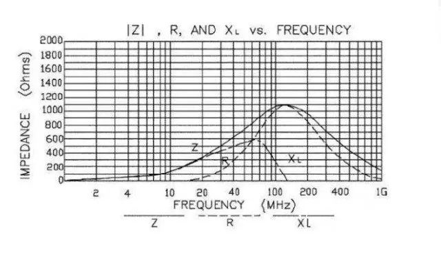
3, the magnetic beads are very important in the middle of the radiation, the previously used materials are K5A, K5C, the impedance curve of the magnetic beads is related to the size and size of the magnetic core. As shown, the different magnetic beads have different impedance curves for different frequencies. However, the high-frequency clutter is lost and becomes heat (30MHz-500MHz). General MOSFETs, output diodes, RCD-absorbing D, bridge stacks, and Y capacitors can be tested with magnetic beads.
4, input common mode inductance: If it is 2 levels of filtering, the first stage of the filter inductance can consider the sensitivity of about 0.5-5mH, butterfly winding method, 5K-10K material winding, the first level of radiation suppression The effect is good. If it is a 3-core input, you can use a three-layer insulated wire at the input end to wrap around the K5A equivalent material for 3-10 turns. The effect is great.
5, the output common mode inductance, generally using high-conducting magnetic core 5K-10K material, special circumstances can not be changed to K5A equivalent material.
6, MOSFET, the input string of magnetic beads on the drain, the input resistance is increased, DS direct parallel 22-220pF high-voltage ceramic capacitor can improve the radiant energy, can also change the MOS of different current values, or different brands of MOSFET test.
7, the output diode, the set of magnetic beads on the diode can improve the radiant energy. The RC absorption on the diode also has an effect on the radiation. You can also test with different current values or change brands.
8, RCD absorption, C change capacity, R change resistance, D can use FR107, FR207 changed to slow tube, but need to pay attention to the temperature of the slow tube. C in RCD can string small resistance resistors.
9, VCC winding also has a diode, this diode also has a great influence on radiation, generally take a set of magnetic beads, or change the diode to 1N4007 or other slow tube.
10. The most critical transformer. If you can add less shielding, you will be less shielded. If you can't do anything, you can only change the transformer. The copper foil shield inside the transformer has a great influence on the radiation, and the line shielding is the most effective. It is usually changed to the transformer when it is not changed.
11. Efficiency when radiation is rectified. The power supply with the magnetic beads is tested first, and in the case of PASS, the magnetic beads are cut one by one.
In the case of fail, a magnetic loop is placed at the input and output terminals to determine whether the radiated signal is transmitted from the input or the output.
If the magnetic ring or the fail is set, it proves that the radiant energy comes out of the board. At this time, find the lab brother to make a probe to test to see which component radiates the most energy, which one has the highest energy at the frequency point beyond the limit, and then rectify the corresponding components.
The phenomenon of radiation can be regarded as the power device in the case of high-speed switching. The oscillation caused by the parasitic parameters is transmitted on different antennas, and is amplified and displayed by the antenna. To avoid the oscillation signal, it is necessary to avoid high-frequency oscillation and change the oscillation frequency. Or the high-frequency oscillation is absorbed and lost, so that the value is not exceeded when the value is displayed.
There is a need to pay attention to the use of magnetic beads. When MOSFET is used, the MOSFET is preferably K-pin. After the magnetic beads are placed, the glue is fixed. If the magnetic beads are loose, the MOSFET may be short-circuited by conduction. Try to use magnetic beads with space when there is space.
7, PCB stereotypes revised trial production attention attention to details
After the completion of the radiation radiation rectification, the PCB can be shaped. It is best to improve according to the production process requirements, and update the PCB to avoid problems during production.
1. The time to verify the power supply is up, the customer request, the specification. The power sample was taken to the test verification group for testing and verification. If the previous problem is solved, the verification group is ok, and it is ok to get the report by the time.
2. Prepare small batch trial production, go through the process, prepare materials, organize the BOM and provide the prototype to the production department colleagues.
3. Prepare document materials such as certified materials (fuse, MOSFET, etc.) and prototypes and key component lists for certification. The components in the list of key components are generally written by more than 3 suppliers. The certification number must be aligned. If it is wrong, the subsequent audit will have unnecessary trouble. All that's left is some basic communication issues.
When I was certified, I was over-standard when I was certified. I can only export it with thermal paste. Or increase efficiency and reduce the amount of conduction and radiation. This kind of problem is usually left too small when you are doing the test yourself, which is difficult to encounter.
4, the general certification can be obtained in about 2 months. Two months is enough to get the trial production ready.
5, trial production problems: basically have to change the large pad, plug hole size changes, silk screen position changes.
6. The test of trial production is completed according to the rules and regulations of IPS and production line testing.
I have encountered the bare board pressure resistance, but the reason is that the bare board is placed on the green electrostatic skin; also the tape attached to the crease of the Mylar sheet is worn out.
7. Input a power supply with a large capacitor. It is necessary to add one to the test process, and an operation flow for discharging the large capacitor after the test is completed.
8. After the trial production is completed, a trial production summary meeting will be held. The trial production will be PASS, and the PCB can be opened. Mass production is basically not a R&D engineer, and at most it is a substitute material.
9, after finishing a product, write something to summarize, or the lessons, or a bit of failure, or the characteristics of different ICs. The project is much more, and it will be natural.
The entire development process is a team collaboration, so very powerful engineers, communication skills are also very strong, research and development of a
Shenzhen Ousida Technology Co., Ltd , https://en.osdvape.com