In China's range measurement and control field, all data exchange is based on the simplified version of HDLC regulations, so we have developed a communication card based on simplified HDLC regulations. The simplification of the HDLC procedure is mainly to improve the real-time nature of communication. All communication contact command frames in the HDLC procedure are simplified, and only data communication frames are retained to ensure a certain real-time nature. Because the card has high reliability, simple and convenient use, and has the characteristics of intelligence at work, it is widely used in various fields of data transmission in the measurement and control system. At the same time, as the Windows XP operating system is gradually applied in the measurement and control system, it is imperative to develop a Windows XP driver for the communication card. Therefore, we have developed a core state driver for the self-developed communication card. After extensive user use, it is generally reflected that the application is good. The design of the communication card and the design of the driver are introduced below.
Hardware design of communication card
1 The main characteristics of the communication card The hardware design of the communication card is intelligent communication: it has 4 DMA channels and the corresponding data buffer storage area on the card. During the data receiving process, the communication card will automatically receive the frame data, determine the frame length, and submit the received frame data to the system at the end of the frame. In the process of sending data, the system only needs to submit the sent data to the card. The specific sending process is completed by the card itself, and the host does not increase the overhead due to multi-channel communication. The card has two working modes of internal / external clock, modem can be omitted at close range, the baud rate is 600b / s ~ 64Kb / s, and it provides 2 interfaces that comply with RS-232 / CCITT V.24 and RS-422A signal.
2 Circuit design of communication card
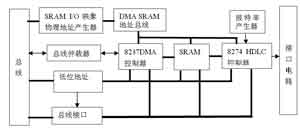
Figure 1 Block diagram of communication card
The block diagram of the communication card is shown in Figure 1. It is mainly composed of DMA controller, bus competition arbiter, serial communication controller, data buffer memory SRAM, memory I / O image and physical address generator, bus interface and protection, baud rate generator, interface circuit and other units Circuit composition.
The DMA controller acts as the master device of the communication card, controls the data reception and transmission on the card (from the communication controller and CPU), and is responsible for arbitration priority. During data communication, the host CPU is allowed to access the SRAM of the card, and when the host sends a control command to one of the channels, it does not affect the other three channels of communication. This will cause the host CPU to compete with the card DMA for the bus control of the card. . The host computer CPU command queuing status sequence is not given on the bus, so multi-master competition cannot be directly designed. Therefore, a state machine is designed on the card bus with a gate array to continuously monitor the bus contention and complete the card bus competition. Dispute and arbitration functions. The device that completes the serial communication of HDLC regulations is the INTEL 8274 multi-procedure serial controller, which can complete two independent serial receive / transmit full-duplex communications. In order to make 4 channels send or receive a frame of data, the host does not intervene, so the sent one frame of data is sent to the SRAM on the card by the CPU with a batch command before the transmission begins; similarly, during the reception process , DMA on the card puts the received data into SRAM, waits for the completion of a frame to be received, and then take out with batch command and put it into the system memory. The SRAM on the card does not occupy the memory address of the host, and uses the I / 0 image. After the adapter is inserted into the host, the host accesses it through the system I / O address. This is done by the address generator. The bus interface includes data transceiver, data switch circuit, read, write and interrupt control circuits, address decoding, etc. The baud rate generator provides a programmable clock signal generator, and the user can set the communication rate by himself for working in the internal clock mode. The interface circuit provides interface signals that comply with RS-232 / CCITT V.24 and RS-422A standards.
3 Communication flow design If you want to send a frame of data, the CPU puts the data into the SRAM of the card with a batch command, and then sets the corresponding sending DMA channel. The DMA channel is a non-automatic reloading method, the 8274 controller is started to send, and then the CPU does not need to be managed, and is automatically sent by the hardware on the card.
If you need to receive data, start the receive channel. The receiving channel automatically searches for input signals. When a data frame is found, it is managed by the DMA controller on the card. The received data is placed in the SRAM of the card, and an interrupt is requested to the CPU to read out the data.
4 Bus contention design Since four channels of communication can be carried out at the same time, and the CPU can send control commands to a certain channel or access the SRAM memory on the card at any time, there will be a situation where the CPU and the card main device DMA compete for the card bus. Because the ISA bus failed to give the CPU instruction queuing status sequence, this brought difficulties to the bus arbitration, and the bus competition and arbitration of this card were completed by the state machine designed by the programmable logic device. The state machine uses a 4MHz signal as a clock and has 3 states:
â‘ CPU control status.
â‘¡ DMA control state.
â‘¢ In idle state, neither CPU nor DMA can get control.
When the state machine detects that there is no CPU and DMA to apply for bus usage rights, it enters the idle state, and once the CPU or DMA requests the bus, the state machine immediately hands over the bus usage rights to the CPU or DMA. If during the CPU control state, DMA is applying for bus use rights, the state machine still determines that the CPU is controlling the bus, leaving DMA in wait until the CPU instruction is detected to complete before the state machine transitions to the DMA control state. If in the DMA control state, the CPU applies for the right to use the bus, the state machine still determines the DMA control bus, leaving the CPU in wait until the DMA bytes are transferred, and the state machine changes to the CPU control state. The use right of CPU and DMA on the bus is a single instruction or byte transfer, and no bus block is set, so the CPU and DMA can frequently exchange the use right, and there will be no phenomenon of waiting for too long.
Driver Design of Communication Card
1 I / O model of the device driver The driver of the communication card is a standard core state device driver developed using the DDK software of Windows XP. It uses a unified "file" form, and users can access it with file operation functions in the WIN32 subsystem by representing the file name of the communication card device. The device driver and program can be set to load automatically or manually according to the needs of users, or the driver can be dynamically loaded. The driver of the communication card is designed to support the synchronous I / O model, which can also be the asynchronous I / O model.
2 The sending data I / O routine is designed to submit the sending task to the core state in the user mode. The I / O management program is responsible for calling the driver. The driver sends the IRP to the hardware. If the current transmitter is not busy, the specific sending operation It is all done by the sender itself, and the driver returns a sign that this frame can be sent. The specific sending completion result can be queried after the sending task is completed. However, if the program submits a send task to the sender of the current device, and the sender is processing the previous frame, then there are two ways to process it.
â‘ Immediate mode: An error is returned immediately. The current device is busy and cannot be sent.
â‘¡ Blocking method: The I / O manager program will schedule the corresponding asynchronous processing routine, put the current sending task into the task queue, and return a flag: I / O hangs, the current device is busy, and the sending task submits the task queue. The driver will submit the sending task in the task queue to the sender when the sender is idle. After the sending task is completed, the relevant file handle is set to a signal state to notify the completion of the sending task.
3 Receive data I / O routine The receive data routine adopts the client / server model design. Because the user's receiving request and hardware receiving are not synchronized, in the design, in order to avoid losing data, consider creating a special receiving thread. In this way, the communication between synchronous user requests, receiving threads, and hardware layers must be carefully designed. Figure 2 illustrates user-mode receiving requests, receiving threads, and communication synchronization between hardware layers.

Figure 2 User mode receiving request, communication synchronization between receiving thread and hardware layer
â‘ Communication between the hardware layer and the receiving thread The synchronization of the communication between the hardware layer and the receiving thread is achieved by synchronizing event objects. The synchronization event object is usually in a no-signal state. Only when a frame is successfully received, the event is placed in a signal state. The receiving line waits for the synchronization event object for a long time. When no data is received, the synchronization event object is blocked because it is in a signalless state. When the hardware detects the data, the real-time interrupt service program is responsible for placing the synchronization event object into a signaled state, and the receiving thread will release the block. Read the received data on the SRAM of the communication card into the receiving thread buffer queue, and then set the synchronization event object to no signal state. The receiving thread blocks again and waits to receive the next frame of data.
â‘¡ Communication between the user layer and the receiving thread When the user submits the receiving task, the driver's scheduler reads the buffer queue of the receiving thread and sets the flag to "empty", and sets the buffer queue event to no signal Status and return, if the buffer is empty, then â— Immediately: no data is returned immediately.
â— Blocking mode: block until a data queue enters. Each buffer of the receiving queue corresponds to a notification event. If the receiving thread reads the data in the SRAM into the queue, the corresponding notification event is set to a signal state, and the user requests to wait for the notification event, as long as there is data in the queue In, it reads and returns, otherwise it is blocked.
4 Hard interrupt service program design The communication card has real-time performance in full-duplex communication, and at a higher baud rate, there are many hard interrupts. In order to prevent high-priority interrupts from preempting CPU time too much, the design uses real-time interrupt service routines and methods of delaying process calls.
In the Windows XP system, each kernel function and process runs at a specific priority. Higher priority functions or events can preempt lower priority, and vice versa. The real-time interrupt service program ISR runs at the DIRQL level and has a higher priority. It can only be preempted by higher-level hard interrupts and will not respond to hard interrupts of the same level or lower priority. Therefore, in the real-time interrupt service program, only the minimum necessary work is done, that is, the interrupt vector is read out, and a large amount of data transmission and processing are handed over to the delay process DPC to complete. Because the DPC process runs at the DISPATCH_LEVEL level, which is a relatively low priority, it can be preempted by any level of hard interrupts. In this way, not only ensure the timely response of the hard interrupt, but also improve the performance of the program.
5 Driver entry routine
Windows XP provides a default standard entry point DriverEntry () for each kernel state driver. In the design, considering that this routine runs at the level of PASSIVE_LEVE, the system only discards this routine once, so important data and objects used in the driver cannot be saved in the DriverEntry () routine. A NoPaged memory is allocated to save during initialization. The DriverEntry () routine of the driver of the communication card mainly completes the following functions.
Read the Registry hardware configuration information; declare I / O addresses, interrupts, and other resources; create a device name MPSC representing the communication card, which is visible to the WIN32 subsystem; set the entry point of the dispatch routine; allocate a NoPaged memory, Store important information; connect hard interrupts, set interrupt service routines; initialize kernel objects such as threads, events, semaphores, DPC; return status STATUS_SUCCESS.
If you encounter an error in the above process, you need to do the following: disconnect the hard interrupt; release hardware resources; package and record the relevant error information; return the error information.
6 Problems that need to be paid attention to in designing the driver program Because the communication card has a certain real-time performance in the application, in order to overcome the uncertainty of interruption and improve the performance of the system, the most difficult asynchronous driver program among all the driver programs of the Windows XP system was developed. In the development of the kernel of the system and the asynchronous model I / O operations, the synchronization of kernel objects is very complicated, and slight errors will cause the system to completely crash. Need to pay attention to the following problems in designing the driver.
â— Kernel objects used in the program: events, semaphores, threads, spin locks, etc., must be stored in Nopaged memory, otherwise, it will cause the system to crash.
â— In the DPC routine, if you want to access the port address used in the interrupt service program ISR program, you must put the access statement in the synchronization routine provided by the system, because when the DPC routine accesses the port, it is possible It is preempted by the ISR routine with a higher priority and causes data errors.
â— The driver must not access the runtime functions of the WIN32 subsystem.
Automobile device for giving light, especially one that has a covering or is contained within something. Lighting should be provided with good lighting and should minimize glare. For the headlamp, in order to meet the above two requirements, use the two conditions of distant light and near light. The distant light is a long distance light beam that is used in the front of the car or not following other cars. It is generated by the main filament in the focal point of the reflector and the power is large, and the beam direction is approximately horizontal. In order to ensure the safety of driving, the distance of light distance (detection and identification of obstacles) should be greater than the braking distance to realize the timely parking. The speed limit is applied in most countries, given that the required distance light intensity is proportional to the four times of the speed.
Auto Lamp
Auto Lamp,Auto Car Head Lamps,LED Combination Tail Lights,Multifunction Auto Lamps
Heshan Jianhao Lighting Industrial Co., Ltd. , https://www.sunclubtw.com