In this paper, a single-chip DSP device TMS32F2812 is adopted. Through the research on the demodulation algorithm of the orbital frequency shift signal, the design system has the advantages of high integration, good real-time performance, strong anti-interference ability and high reliability.
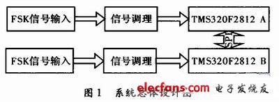
1 overall design of the system
The system uses the TMS32F2812 processing chip with a frequency of up to 150 MHz and a clock period of 6.67 ns. 2&TImes; 8 ADC conversion channel. SPI serial port. Two modules, 1 kb & TImes; 16 SARAM, which are easy to implement the large-capacity SARAM space required for ADC sampling, master-slave control chip data exchange and FFT conversion.
The overall design of the system is shown in Figure 1. With dual-system hot standby, the two channels simultaneously sample and demodulate the conditioned FSK signal and compare the output to improve the reliability of the system.
2 main technical realization
2.1 Signal Conditioning
The signal conditioning mainly uses a low-pass filter. The design of the low-pass filter uses the software FilterLab designed by the MicroChip filter. The software only needs to input the passband frequency and the order of the filter to generate the corresponding circuit diagram, eliminating the need to save the corresponding circuit diagram. Complex operations in filter design. Figure 2 shows the Butterworth low-pass filter generated by FilterLab software with a factor of 4 and a passband frequency of 4 000 Hz. The recommended values ​​for the filter capacitance are given.

2.2 Signal sampling design
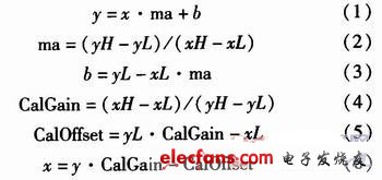
Due to the internal A/D of TMS320F2812, in the actual operation, the internal A/D sampling error is found to be large, up to 9%, which is far from the sampling accuracy requirement and needs to be corrected by software. First, select any two channels of the ADC as the reference input channel, and input the known DC reference voltage respectively. Obtain the conversion value by reading the corresponding result register. The correction gain and correction of the ADC module can be obtained by using the two sets of output values. Offset, then use these two values ​​to compensate for other channel conversion data. The specific compensation formula is as shown in equations (3) to (6).
132Kv Transformer,132Kv Power Transformer,132Kv Power Transformer With Oltc,132Kv Transformer With Oltc
Hangzhou Qiantang River Electric Group Co., Ltd.(QRE) , https://www.qretransformer.com