 The following is the circuit diagram of [LTC2752 pin function diagram and application]
 Features 6 output ranges are available through programming or pin bonding:
0V to 5V, 0V to 10V, -2.5V to 7.5V, ±2.5V, ±5V, ±10V
Maximum 16-bit INL error: ±1LSB over temperature
Monotonic interference pulses are guaranteed over the entire temperature range: 0.6nV•s (3V), 2.2nV•s (5V)
Serial readback of all on-chip registers
1μA maximum supply current
2.7V to 5.5V single supply operation
16-bit settling time: 2μs
Voltage-controlled offset and gain trimming to 0V and power-on reset to 0V (this is independent of the output range)
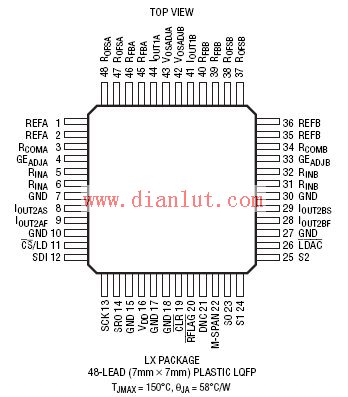
48-pin 7mm x 7mm LQFP package
Structure block diagram:

The LTC2752 is a dual, 16-bit multiplying serial input, current output digital to analog converter. The device operates from a single 3V to 5V supply and guarantees monotonicity over temperature. With no adjustments, the LTC2752A provides full 16-bit performance over the entire temperature range (±1LSB INL and DNL maximum). The SoftSpanTM DAC provides six output ranges (up to ±10V) that can be set via the 3-wire SPI serial interface, or pin-bonded to operate in one output range.
Any on-chip registers (including the DAC output range setpoint) can be read in one instruction cycle for verification; and if you change the contents of the register, the changed register will be in the next instruction cycle. Automatically read back.
The device also provides voltage-controlled offset and gain adjustment; moreover, both the power-on reset circuit and the CLR pin reset the DAC output to 0V, regardless of the output range.
(Editor: Circuit Diagram)
Shenzhen E-wisdom Network Technology Co., Ltd. , https://www.healthy-cigarettes.com