Main features
Applications that operate on a lithium battery
Output voltage can be set with pins
With synchronous rectification function to improve efficiency
Using small ceramic capacitors
Using ultra-small micro SMD-10 package
Although there are many different buck converters on the market, most of them cannot meet the requirements of portable device manufacturers due to the large package and insufficient accuracy. To meet the market demand in this regard, National Semiconductor recently introduced a series of buck converters with smaller packages, higher performance, and more complete functions, including LM2608, LM2612, LM2614, and LM2618. This series of chips are packaged in micro SMD-10, with an area of ​​only 2.25 mm x 2.504 mm and a height of 0.6 mm. This series of products is more compact than other manufacturers' products that only use SOT-23 package. National Semiconductor's micro SMD package is the industry's smallest package. This package uses innovative technology to make its die can be imported into the package. The thermal resistance (qJA) of this package is 140 / W, which is superior to the 250 ° / W thermal resistance of the SOT-23 package. Due to its excellent thermal conductivity, its chips can dissipate heat faster, which helps improve efficiency. The micro SMD package occupies less board space, and its small size makes it the most ideal package.
Buck converter chip output voltage mode synchronous pulse frequency modulation (PFM) output current
LM2608-1.31.3 volt (V), 1.5 volt pulse width modulation (PWM) / low voltage drop (LDO) 400 mA / 3 mA
LM2608-1.81.5V, 1.8V pulse width modulation / low voltage drop 400 mA / 3 mA
LM2612 BL / TL 1.05V, 1.3V, 1.5V, 1.8V
Pulse width modulation / Pulse frequency modulation (PFM) 400 mA / 100 mA
LM26141.0V to 3.6V (adjustable)
Pulse width modulation / pulse frequency modulation 400 mA / 100 mA
LM2618 1.8V, 1.83V, 1.87V, 1.92V pulse width modulation / pulse frequency modulation √400 mA / 100 mA
National Semiconductor's series of buck converters are most suitable for digital applications such as mobile phone baseband processors, RF power amplifiers, and PC cards. This series of chips can provide an input voltage of 2.8 V to 5.5 V, can be operated with a lithium battery, and use the pin to set the operating mode, the accuracy of its output voltage is 1% to 2%, and the ripple is extremely low (When the pulse width modulation mode is used, the ripple is generally only 5 mV). Figure 1 lists several buck converters suitable for power management solutions for portable devices.
Older mobile phones use batteries to directly drive the power amplifier, so the efficiency is lower. As long as we adjust the supply voltage of the RF power amplifier according to the required transmission power, we can improve the transmission efficiency and extend the battery life. Figure 1 is a typical application circuit for driving an RF power amplifier, which uses the LM2614 chip. The output voltage of the LM2614 chip can be flexibly adjusted at any time within the range of 1 volt to 3.6 volts. The actual output voltage is controlled by the digital / analog converter signal issued by the baseband processor. The built-in features of this chip include a fast output slew rate of no more than 30 ms for the conversion stage from the lowest output voltage to the highest output voltage, and a duty cycle of up to 100% (to make full use of the battery's available voltage range) , And high efficiency (see Figure 2). The LM2614 chip can also provide a fixed output voltage.
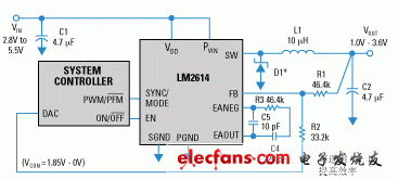
Figure 1: Typical application circuit of LM2614
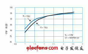
Figure 2: LM2614 high efficiency curve
Figure 3 shows the typical application circuit of the LM2618, while Figure 4 shows the typical efficiency curve of this chip when it uses pulse frequency modulation (PFM) mode for rectification. National Semiconductor is about to launch a buck converter that can output a lower voltage for selection. LM2608 / 12/18 The three chips all contain digital-to-analog converters. You only need to input the logic signal to the VID pin to set the output voltage, so there is no need to install a feedback resistor divider to ensure the output of the pulse frequency modulation mode. The voltage ripple can be kept at a low level, and it also ensures that the voltage can be flexibly changed, which is an important feature of the intelligent power management system. In addition, these three chips also have other built-in functions, including internal compensation, low shutdown current (typical value is 0.02mA), frequency synchronization, current limit protection, overheat shutdown protection, internal soft start, and output voltage high protection .
In addition, the system controller can select operation modes such as pulse width modulation (PWM), pulse frequency modulation (PFM), and low pressure drop (LDO) through pins to extend battery life and reduce noise interference. This design, which can actively select the operation mode, allows system design engineers to directly intervene in the process of mode conversion, which is superior in design to the automatic conversion mode according to the magnitude of the load current, because the automatic conversion mode may interfere with the operation mode of the system.
These three chips have strict tolerance limits on the oscillator frequency, and the tolerance of the conversion peak current limit is extremely small. For example, the tolerance of the LM2608 is 15%, and the tolerance of the LM261x series is 20%. This design improves electromagnetic compatibility and allows the system to use smaller inductors. If the load current is high, internal synchronous rectification and low on-state resistance (RDSON) metal oxide semiconductor field effect transistor (MOSFET) and pulse width modulation (PWM) operation modes can be provided to maintain high efficiency operation. Its quiescent current is as low as 180mA, so the low-power pulse frequency modulation mode can ensure that the conversion efficiency can be maintained at a high level under very weak load current. Low-voltage drop (LDO) mode can ensure that the system can be started at any time when it enters the standby state, so as to resume operation, and the system consumes only 20mA of current after entering the standby state. These converter chips use smaller ceramic capacitors, which is an important functional feature. The LM2612 / 18 only needs three small surface-mount external components to support it.
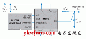
Figure 3: Typical application circuit of LM2618
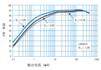
Figure 4: Typical efficiency curve of LM2618
Silicone Keychain/Key Ring introduction:
Do you have many keys on hand ?For household ,for office ,for cars to lock and open?Definately ,everybody has keys! To keep our keys in order ,we will need to buy a keychain ,to make our life more colorful and interesting ,maybe if there is some cartoon images will be very funny,our company help you to do silicone keychains by your own design and assemble with stainless rings,this make your keys more flexible and the ring can avoid being rust!
Silicone Keychain/Key ring description:
1.Product name:Silicone keychain,custom silicone keychains,customized 3d Silicone Keyring,keyring silicone,silicone rubber keychain,Keychain Silicone
2.Place of origin:Guangdong China
3.Color:any pantone color is available
4.Logo:printing,debossed,embossed .
5.MOQ:500pcs.
6.Package:1 pcs/opp,customized design is available.
7.Design:Customized
8.Certification:FDA,LFGB,SGS,ROHS,etc.
9.Usage:Gifts/collecting keys
10.Some Silicone Keychain/key ring photos for ref.

Silicone Keychain/Key Ring
Silicone Key Chain,Custom Silicone Keychain,Keychain Silicone,3D Silicone Keychain,Silicone Keyring,Silicone Key Ring
OK Silicone Gift Co., Ltd. , https://www.oemsiliconegift.com