This design is mainly composed of the following three parts:
First, the audio chip CXA1691, which is an AM/FM stereo radio IC integrating amplitude modulation, frequency modulation, phase-locked loop, stereo decoding and other circuits. Second, the phase ring chip BU2614, through a reasonable design of the loop filter, the frequency can be stabilized at 88 ~ 108MHz. Third, the DC-DC conversion circuit realizes low power consumption and single power supply of the system.
System hardware circuit design
1 receiving circuit design
The CXA1691S has a wide supply voltage range, and the circuit can work normally in the range of 2 to 10V. In addition, it also has stereo indicator LED driver circuit and FM squelch. Since the system does not involve amplitude modulation, the 16-pin (AM IF input), 15-pin (band selection), 10-pin (AM antenna input) and 5-pin (AM local oscillator) in the chip are all suspended. Can be connected to the ground. The 7-pin (FM local oscillator) and 12-pin (FM input) are connected to the input of the loop filter to control the frequency with a phase-locked loop. The specific circuit is shown in Figure 1.
This article refers to the address: http://
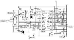
Figure 1 CXA1691 radio circuit
2 Phase-locked scheme design The second major part of the design is the design of the phase-locked loop circuit. The following options are considered here.
Solution 1: The D/A control voltage controlled oscillator is used to generate the variable local oscillator frequency. The tuning mode of the scheme is relatively simple, and the automatic search function can be easily realized, and the frequency can be finely adjusted to achieve the best sound receiving effect. Debugging software by debugging software makes debugging relatively easy. But it also has two shortcomings: First, the signal amplitude generated by the DAC is quantized, and the local oscillator frequency cannot be accurately locked; second, there is no loop control, and the stability is not as good as the phase-locked loop. However, the control voltage can be stepped to 20mV by using an 8-bit DAC. If a 12-bit DAC is used, the control is more accurate. It can be seen that the above two disadvantages can be overcome.
Option 2: Adopt PLL frequency synthesis method. PLL frequency digital tuning system is mainly composed of voltage controlled oscillator (VCO), phase comparator (PD), low pass filter (LE), programmable frequency divider and high stability crystal oscillator. Its structure is shown in Figure 2. . The reference divider, PD, and programmable divider can all be integrated inside the chip BU2614, and the VCO oscillator outputs fosc as the local oscillator frequency. The BU2614 can be controlled by a microcontroller. The high stability crystal oscillator greatly improves the stability of the local oscillator frequency, and the frequency stepping scan, preset radio station, radio storage and other functions can also be realized by controlling the frequency division coefficient by the single chip microcomputer. 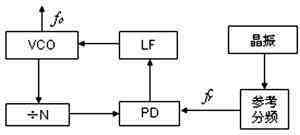
Figure 2 phase lock schematic
The above two schemes are widely used in current product design. In order to stabilize the radio reception effect and realize the continuity of automatic search, the design adopts scheme 2, and the circuit is shown in FIG. 3.
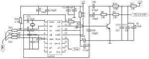
Figure 3 phase-locked loop circuit
3 Power Supply Design Another feature of this system is the design of the DC-DC converter circuit. After trying many methods, the MAX770 is finally selected as the 3V to 5V power supply, which can output +5V. The current meets the design requirements at 1A, and the ripple is small, less than 100mV. If filtering is used, the effect is better. Its circuit is simple, the output voltage is also quite stable, and the circuit is shown in Figure 4.
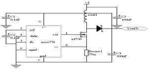
Figure 4 3V to 5V power supply design
4 Clock display The DS12887 real-time clock chip used in this design is made of CMOS technology. It has internal crystal oscillator and clock chip backup lithium battery, and is compatible with the commonly used clock chip MC146818B and DS1287. The clock circuit designed with the DS12887 chip does not require any peripheral circuits and devices, and has a good microcomputer interface. The chip contains 128 bytes of RAM unit and software interface, 14 bytes are clock unit and control / status register, 114 bytes is general purpose RAM, can be used by users, all RAM unit data has power-down protection, can be used to achieve The function of electrical storage.
This system has other very special features, such as automatic search locks and power-down storage.
Conclusion This design is a simple and practical FM receiver solution. The application of CXA1691 greatly reduces the complexity of circuit design, and it integrates most of the circuits to enhance the stability of the system. I have used the NE564 and some auxiliary circuits to design the radio circuit. The sensitivity and signal-to-noise ratio of the radio are not comparable to this design. In addition, it integrates an audio power amplifier circuit to make a qualitative leap in sound quality.
The design of the phase-locked loop circuit is critical in this design, especially the design of the loop filter. I tried the triode circuit and tried the combination of LM358 and LC circuit. Finally, the design of the scheme was determined from the bandwidth and stability.
Copper Connecting Nose,Cable Nose,Cable Terminal
Cutout Fuse Co., Ltd. , http://www.nsindoorfuse.com