Today, touch panels are indispensable input devices for tablet terminals and smartphones. With the appearance of "Windows 8" in the fall of 2012, the touch panel also began to be used as the user interface (UI) of personal computers. In shopping malls, etc. in Japan, there is a trend to use large touch-panel displays larger than 30 inches in the floor guides and Table PCs. This field is called digital signage, and the market is constantly expanding. The use of touch panels is increasing, and it is expected that the market size of displays with touch panels in Japan will exceed 2 trillion yen around 2015.

However, large touch panels have technical issues in terms of cost and performance. The Touch Panel Research Institute has developed a transparent conductive film "SpiderNet" that can fully exhibit the performance of products larger than 10 inches by forming copper wiring on a PET film substrate, and has been shipping since December 2011. This article will introduce the development background and the characteristics and characteristics of the development products.
ITO is dominant in products under 10 inches
At present, touch panels of 10 inches or less used in smartphones, tablet terminals, etc. are mainly electrostatic capacity type, and the touch panel unit adopts a “discrete type†provided as an independent external component (Figure 1). This touch panel is mainly divided into a type using an ITO glass substrate on a sensor substrate and a type using an ITO thin film substrate. "IPhone" and other ITO glass substrates are used, and "iPad mini" uses ITO thin film substrates. The market is currently divided into two major fields of resin films and glass.
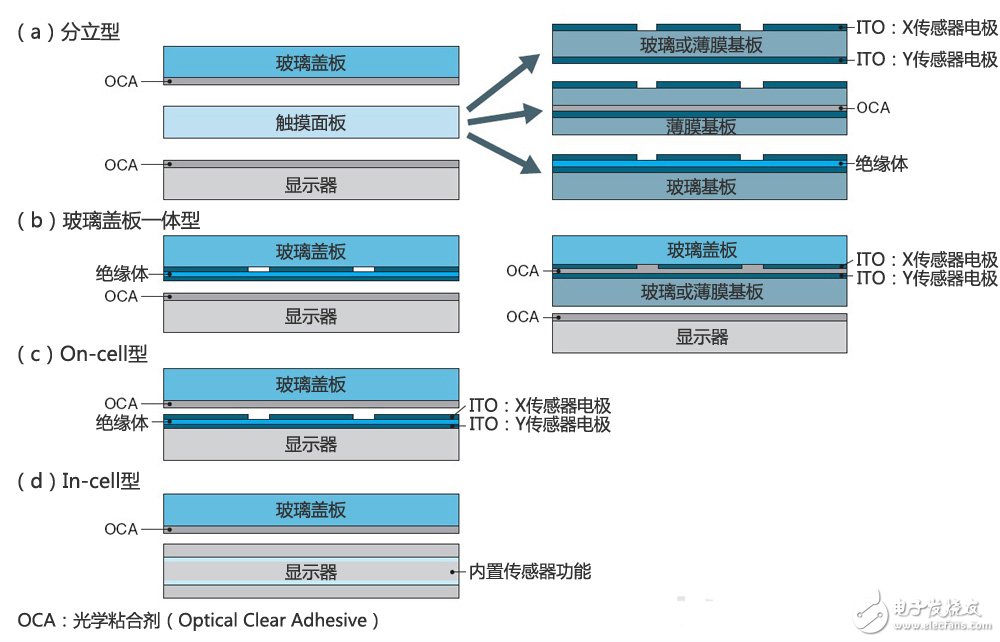
Figure 1: Classification based on the cross-sectional structure of the touch panel
At present, (a) discrete type is the mainstream, but for the new generation of products, (b) integrated glass cover and (d) In-cell type are also increasingly active.
For the new generation of products, the current development trends include the "OGS (One Glass SoluTIon) type" (also called integrated glass cover type) equipped with a touch panel function on the glass cover that covers the surface of the product casing, and the display unit "In-cell type" embedded with touch panel function. For the OGS type, the ITO layer is formed on the entire chemically strengthened glass cover plate and then cut into single sheets. The most promising mass production method, but there are still problems with the method of cutting strengthened glass and its yield. In order to solve this problem, achieve light weight and reduce costs, the "OPS (One PlasTIc SoluTIon) type" has attracted attention. That is, the trend of replacing the glass cover with a resin protective film, the high-heat-resistant resin film to be mentioned later is one of the candidates.
For the In-cell type, "Sony's product" uses the anti-static ITO layer on the color filter substrate for the sensor electrode, while Apple Inc. of the United States uses X and Y sensors formed on the TFT substrate for the "iPhone5". Autonomous way of electrode. Both methods share the drive circuit in the touch panel and the liquid crystal panel, so it is necessary to synchronize the drive of the touch panel and the liquid crystal panel. Therefore, as the size of the product increases, the ratio of display writing time increases, and it is difficult to secure the touch detection time.
Increased size and decreased responsiveness
In addition to these issues, when the screen size is expanded to more than 10 inches, there will also be issues in terms of materials. One is that the resistance of current ITO sensor electrodes becomes too large, and the other is that the number of electrodes increases and the area of ​​the frame wiring portion increases.
In order to achieve multi-touch and achieve a certain degree of position accuracy, the capacitance type touch panel needs to reduce the distance between the sensor electrodes from the current 6mm to about 4-5mm. To meet the performance parameters of Windows 8, the line spacing below 5mm is required. As the screen size expands, the number of sensor electrodes will inevitably increase. For example, the Windows 8 performance parameters of a 20-inch screen require a total of 150 X-electrode electrodes and Y sensor electrodes, and 150 wires for wiring. In order to narrow the frame portion where wiring is provided as much as possible, it is necessary to reduce the line width / line distance of the wiring to about 30 μm / 30 μm, and to reduce the resistance value as much as possible.
In addition, as a basic element of the characteristics required for the transparent conductive film of the capacitive touch panel, the resistance between the sensor electrode terminals can be reduced to 10 k to 15 kΩ or less. This is a requirement of semiconductor manufacturers supplying sensor driver ICs.
The background of this requirement will be described below by taking the prismatic pattern sensor electrode shown in FIG. 2 as an example. The circuit is composed of two parts: resistance (R) and capacity (C), and the time constant (signal rise time) τ of the circuit is represented by τ = R & TImes; C. The signal change at the time of finger touch also operates according to this time constant. Therefore, in order to detect the signal within the allowable time of signal detection (approximately μs), R = 10k to 15kΩ or less is required. In the prismatic pattern of FIG. 2, when the resistance value between the sensor electrode terminals is 10 kΩ, the relationship between the panel size and the required resistance value of the ITO film thin film can be obtained.

Figure 2: The size of the touch panel and the film resistance of the ITO film required
The thin film resistance value of the widely used ITO film is 140Ω / □, which is not suitable for touch panels of 10 inches or more that require a resistance value of less than 100Ω / □.
From the calculation results, it can be found that the 10-inch touch panel needs to suppress the ITO film resistance to about 100Ω / □, and the 40-inch large touch panel needs an ITO film of 20Ω / □. Of course, the final result varies depending on the pattern shape of the sensor, but the relationship is the same. Among the commercially available ITO / PET films, Nitto Denko ’s 140Ω / □ products are the most widely used materials, and 100Ω / □ products are still in the sample supply stage. The touch panel of about 10 inches is also made of ITO and PET film, but it is dealt with by taking out the wiring electrodes at both ends of the long-side sensor electrodes.
On the other hand, ITO glass can heat the glass substrate to nearly 300 ° C during the ITO film formation, so it can reduce the resistance compared to the thin film substrate, and a transparent conductive film of about 20Ω / □ can be obtained. However, in order to reduce the resistance, it is necessary to increase the film thickness of the ITO layer. Therefore, the light yellow color peculiar to ITO is very dazzling. Even a resistor that can be used with a thinner film thickness cannot be used because the ITO layer interferes, which results in a decrease in transmittance. The glass substrate is heavy and easily damaged, and it is not easy to handle when it is enlarged. That is to say, the large-scale touch panel is suitable for using a thin film substrate.
* Open bottom = naked eyes can see the change of material.
We are engaged in manufacturing and supplying a wide range of Transformer Bobbins which is highly used for effectual functioning. Our bobbins are manufactured using quality material such as nylon, polycarbonate and ld. These are used as suitable storage for wires in the shape of coil. Further, these are widely applicable in electronic industry and are offered as per the desired requirements and specifications of our clients.

Transformer Bobbins,Plastic Transformer Bobbins,Pot Core PC Bobbin,EFD-15 Surface Mount Bobbin,Bobbin E-Core
NINGBO BEILUN TIAOYUE MACHINE CO., LTD. , https://www.spool-manufacturer.com