Field programmable gate array (FPGA) chips are widely used in network devices, communication devices, industrial systems, and automotive electronic systems. Because the FPGA chip has a high degree of flexibility in practical applications and also has a reconfigurable feature, it has become an indispensable basic component of the above-mentioned various electronic products. Recently, the application scope of the FPGA chip has been further expanded. It has even been widely applied to various electronic consumer products such as set-top boxes, DVD recorders, and electronic game consoles. It is expected that the application scope of the FPGA chip will be further expanded, and it is believed that there will be further growth in the applications of global positioning systems, medical equipment, measuring instruments, and portable devices.
Why did engineers designing portable and handheld electronic products use FPGA chips instead? The reasons are many, such as continuous improvement of process technology, power consumption and cost of the chip is also greatly reduced, and the volume becomes smaller and smaller. However, if the portable electronic products use FPGA chips, power management will become a big problem for the system.
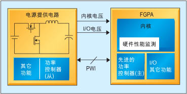 |
Figure 1: Schematic diagram of advanced voltage regulation. |
Different systems have different requirements on the power supply, and it is important to understand this because the input voltage of the power supply, complex startup conditions, transient response, and power supply sequence must be resolved. FPGA chips require multiple different supply voltages, such as core voltages (0.9V to 2.5V), I/O voltages (2.5V to 3.3V), and low noise, low ripple voltage (typically 2.5 V or 3.3V). In addition, if the power supply of the FPGA chip comes from the battery, the problem of system efficiency and battery life becomes extremely important.
FPGA Power Management Challenge
No matter what type of FPGA chip is used, the final system determines what kind of power challenges will be faced. For example, DVD recorders that can receive satellite broadcasts need to provide dozens of other voltages in addition to powering the FPGA. For such a system, the size and efficiency of the power supply are not the most important considerations, and the most important thing is to reduce the cost. But for battery-powered systems, efficiency must be greater than everything else.
The efficiency of portable electronic products in use and in standby is very important, because efficiency will directly affect the battery life and length of work. Take a battery-powered system as an example, the input voltage is generally between 1.8V and 5.5V. Most of these products use two AA batteries or one lithium battery as the power supply, and the voltage of these batteries is mostly between 3V and 4.2V. The general operating current will not exceed 1.5A, and most systems require no more than 600mA. Although there is a general set of guidelines for powering an FPGA with which buck converter solution is used, portable electronics have its unique requirements that, even in standby, the efficiency must be maintained at a high level in order to extend the battery life.
For portable systems, a synchronous step-down DC/DC converter is an ideal power supply solution for FPGA chips, and it is ideal for even low load current efficiency. However, the general DC/DC converter has a disadvantage. For example, when the load is small, the efficiency is greatly affected. The advantage of synchronous step-down DC/DC converters is that even if the load is in a "full power" state or the operation is completely stopped, there is no major impact on efficiency because the converter's functionality can be turned off. Since the FPGA chip is powered on standby, the converter will continue to operate at the highest switching frequency while powering the FPGA chip in the standby state, resulting in unnecessary power consumption. Converters used in portable systems must be pulse-skipping or pulse-frequency modulation (PFM) mode so that they can be used in standby mode.
A typical fixed-frequency synchronous buck converter operates in continuous conduction mode, its operating frequency will be fixed, but if you work in PFM mode, the converter has greater flexibility, such as when the load current is reduced, you can Switch to a variable frequency, fixed on-time operating mode and use a discontinuous mode of operation to reduce switching losses.
This kind of converter has a built-in comparator that can sample the output voltage (VO) at a fixed frequency (fPFM) and then compare this output voltage with the reference voltage (VREF). If the output voltage is lower than the reference voltage, the converter will use the pulse. The wide modulation (PWM) mode generates a fixed on-time pulse to charge the output capacitor.
The converter will continue to operate in PFM until the output current exceeds a certain threshold. After this threshold is reached, the converter will operate in PWM mode again. When the load is small, there are two major advantages of using the PFM mode of operation. First, when the PFM mode is used, a large number of internal circuits are turned off, so that the DC/DC converter's power supply current will be drastically reduced; in addition, switching is performed only when necessary. Work, so the switching loss of the output stage can be minimized.
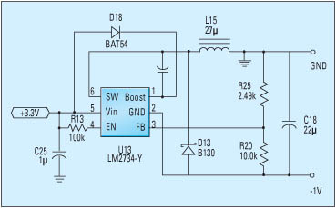 |
Figure 2: This circuit can generate negative voltages to provide reverse bias for the FPGA. |
Engineers designing FPGA power systems should carefully select power management ICs to ensure that the system can maintain high efficiency operation even at full load or minimal load. In addition, the quiescent current of the chip must also be low enough to ensure that power consumption can be minimized when using standby mode.
The core voltage rises monotonously
After the system shuts down, some FPGAs, ASIC cores, and even processors keep the voltage low, which leads to pre-bias conditions. At this pre-bias condition, the power converter enters this voltage at startup. The occurrence of pre-bias causes the converter to have undesired voltage changes at start-up, and the voltage converter does not handle this load condition. The existing voltage present in the converter leads to a reduction in the output voltage at start-up, which is a particularly disadvantageous effect for the converter. The supply voltage must gradually rise steadily until it rises to its rated value. We call this rise in a monotonically increasing voltage. To ensure that the FPGA internal cells start up in the proper way, the supply voltage must rise monotonically. Since these internal units are started during the voltage rise, the "load" faced by the power supply system is not constant. Because of this, the selected converter must be able to regulate its output voltage whether it is in a steady state or a voltage rising phase.
There are currently two ways to ensure that the voltage can rise monotonically. One of the methods is to increase the capacitance of the converter high enough to retain sufficient charge at the output so that the output voltage does not fall during startup. If this method is used, additional large-capacity capacitors need to be added, which will increase the board size and increase the system cost. Another method is to turn off the low-side MOSFET of the synchronous converter, and then monitor the voltage of the switching node when the high-side MOSFET is turned off. The converter will remain in a pre-biased state until after a round of detection, the voltage at the switching node (at the output inductor and the junction of the two MOSFETs) is found to be below 0V during the entire off-time of the high-side MOSFET. The low-side MOSFET must start switching after this condition occurs.
Adjust voltage to increase efficiency
FPGA basically belongs to CMOS chip, its characteristic can be more and more compact with the improvement of craft technology. Because the semiconductor technology of FPGA has been reduced to below 90nm, and the working frequency is rising constantly, the dynamic and static power's size becomes more and more important. The current approach to FPGA design implementation is limited by its design and it is difficult to reduce dynamic or static power, although this is theoretically possible.
The dynamic power can be calculated using the following formula: N in the formula refers to the switching activity of the FPGA, C is the capacitance, f is the frequency, and VDD refers to the supply voltage:

Static or leakage power is caused by three kinds of leakage current: sub-threshold leakage current (Isub), drain-drain-body junction leakage current (Ij), and source-substrate leakage current (Ib) ). Static power can be calculated using the following formula:
![]()
The Vbs in the formula refer to the substrate bias.
Portable power systems require a small form factor and a long battery life. Therefore, simply increasing the power density of the battery or improving the power supply efficiency will certainly not meet these two requirements. For such systems, "dynamic or adaptive voltage regulation" and "reverse bias" are indispensable technologies for reducing processor power. The basic theory behind it can be derived from the above formula. To reduce the processor's dynamic power consumption, we must not only reduce the clock frequency as much as possible, but also reduce the core supply voltage required by a certain clock frequency as low as possible. This open-loop technology is called dynamic voltage regulation (DVS) technology, and adaptive voltage regulation (AVS) technology is a closed-loop control technology, and its performance is much improved than DVS technology. AVS technology can compensate for the effects of different processes and temperatures, and does not require a frequency/supply voltage lookup table like the DVS, which simplifies the voltage regulation method. Hardware performance monitoring circuits used by FPGAs or digital processors can be connected to power controllers through the PowerWise Interface (PWI), which has become an open standard in the industry. And at any frequency, it can operate with supply voltages as low as it can no longer be low.
To add the reverse bias circuit to the circuit shown in Figure 2, a voltage of -0.8V to -1.5V can be input to the substrate of the chip. This can increase the voltage threshold of the chip and reduce the subthreshold leakage to reduce the static power. The purpose of consumption.
Fenghua Ceramic Chip Capacitors
Fenghua Capacitor,Ceramic Capacitors Smd 10V,Ceramic Capacitors 4.7Uf 10V,Fenghua Ceramic Chip Capacitors
JINGGANGSHAN MEICHENG ELECTRONIC TRADING CO.,LTD , https://www.meicheng-tra.com