The embedded image detection system based on FPGA is widely used in industrial field due to its fast processing capability and flexible programming. Usually these systems collect the image data stream and process it in real time to obtain the required feature information. . The acquisition of image data is the first step of the whole system. As the front end of the whole system, it determines the quality of the original data and is the key to the success of the whole system. CMOS image sensor adopts CMOS technology, which can integrate image acquisition unit and signal processing unit on the same chip, which has great advantages in integration, power consumption and cost, which makes its application in embedded image processing. The more you come. Most of the CMOS image sensor chips use a subset of the I2C bus as a control interface. The user can easily program the chip and configure the image sensor internal register data according to the design requirements to obtain the desired image. Taking the MT9P031 image sensor of ApTIna as an example, the interface circuit of I2C bus is designed with Verilog hardware description language. The FPGA is used as the core controller to realize the initialization operation of MT9P031. It not only verifies the configuration effect of I2C bus, but also obtains ideal. Image data also lays the foundation for the processing system of subsequent line structured light images.
1 I2C bus protocol and MT9P031 configuration process introduction
1.1 I2C bus protocol
The I2C (Inter-Integrated Circuit Bus) bus is a two-wire bus developed by PHILIPS for connecting between chips. Due to its small number of interface lines, simple control method, and high communication rate, it is used in single-chip microcomputers, serial EEPROMs, etc. It is widely used in devices. The I2C bus uses two signal lines for data transmission. One is serial data (SDA, Serial Data) and the other is serial clock line (SCL). Several compatible devices (such as memory, A/D, D/A, LCD drivers, etc.) can share the I2C bus. All devices on the I2C bus are addressed by the address signals sent by SDA, and no chip select lines are required. The bus can only be controlled by one master at any time, and each slave initiates a data transfer when the bus is idle.
1.2 MT9P031 configuration timing analysis
Due to the different requirements of the detection system, the image sensor may have to work in different modes, so it is necessary to read and write its internal registers through an external controller to complete the specific configuration. The typical write timing of the MT9P031 register is shown in Figure 1. After the start signal is passed, the FPGA first writes the address 0xBA of the device (ie MT9P031), then releases the SDATA data bus, and then the MT9P031 returns an acknowledge signal ACK. After the FPGA obtains the response signal, After one clock cycle, the register address 0x09 to be configured is transferred, and the 16-bit register data is transmitted after the response signal is acquired. Since only 8 bits of data can be transmitted at a time, the 16-bit register data has to be divided twice to be transmitted. First, the upper eight bits of data are sent, and the last eight bits of data are sent. After each byte of data is sent, the FPGA acquires a response signal from one bit, then ends a transfer cycle and completes the configuration of a register. That is, IDAddress+ SUB-Address + W-Data has a total of 32 bits of data. Repeat the above process to configure different parameters for different registers.
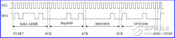
Figure 1 Write MT9P031 timing diagram
2 FPGA module design
In order to achieve the correct configuration of the image sensor, the design must be completed in strict accordance with the configuration timing of MT9P031. In this design, the I2C bus configuration module is mainly composed of three small modules, which are I2C_Clock_Generator, I2C_Controller and Register_Value, and the connections between the modules are as follows. Figure 2 shows.
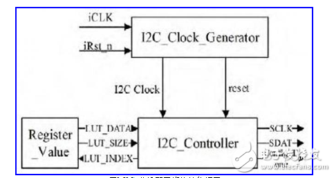
Figure 2 Block diagram of the I2C bus configuration module
I2C_Clock_Generator mainly generates the I2C serial clock signal. There are three speed modes according to the protocol data transmission: normal mode 100Kb/s, fast mode 400Kb/s, high speed mode 3.4Mb/s, in order to ensure the accuracy and success rate of the configuration. The speed mode of 100Kb/ is adopted, that is, the frequency of SCLK is 100KHz. Since the clock input to the FPGA is 50MHz, it needs to be divided by frequency. At the same time, the module is also responsible for generating a valid signal for data transmission, ensuring that the SDAT change occurs during the low period of SCLK.
Register_Value is actually a lookup table, which is responsible for saving the register address and data that need to be configured inside the MT9P031. The number of bits in the lookup table is 24bit. The purpose of being a module alone is to facilitate the user to change the configuration data and determine the different working states of the image sensor. .
I2C_Controller is the core module of image sensor configuration design, which mainly completes the functions of start-stop command generation, byte transmission and reading, and response signal acquisition. At the same time, the I2C_Controller module also generates I2C read and write timing, which is implemented by the state machine in strict accordance with the I2C protocol, and converts the 24-bit opcode I2C_DAT sent from the Register Value part into the correct I2C timing. After the data transfer of a register is completed, the module will also determine whether the register configuration data is sent smoothly. If everything is normal, the LUT_INDEX signal will be automatically incremented to control the Register Value lookup table to generate the address and data of the next register.
3 I2C interface simulation and debugging
In order to verify the correctness of the I2C timing during the MT9P031 configuration process, the design simulates the entire module in the Modelsim Se10.1c software platform, simulates the 50MHz control clock and reset signal in the Test bench, and observes the waveform of the final output. . Figure 3 is a simulated waveform diagram for reading the register address 0x00 of the MT9P031, and Figure 4 is a simulation waveform for writing 0x01EA to the register address 0x01.
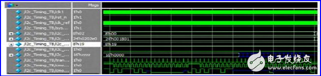
Figure 3 Waveform simulation of reading register 0x00 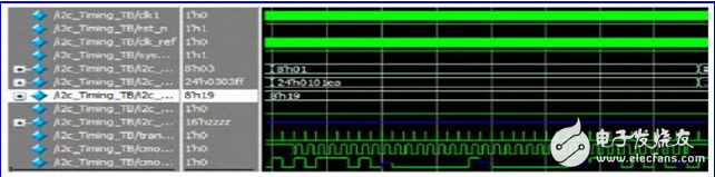
Figure 4 Waveform Simulation of Writing Data 0x01EA to Register 0x01
4 Summary
Image sensor configuration based on I2C bus is very common in video image acquisition and processing system. This design combines the programmable features of FPGA. The modular method design method is used to complete the design of I2C configuration circuit. The design flow of each module is introduced in detail. And the implementation, and finally the entire design was simulated to verify the correctness of the design. After comprehensive debugging, it takes up very little resources and has high reliability. Moreover, the design of Verilog hardware description language makes the portability very strong and has wide application value.
Other Categories,High Quality Other Categories,Other Categories Details, CN
Miraclean Technology Co., Ltd. , https://www.mrccleanroom.com