With the intensification of energy crisis, resource depletion and air pollution, China has established new energy vehicles as a strategic emerging industry. Car chargers are an important part of electric vehicles, and their research has both theoretical research value and important engineering. Value. A block diagram of the vehicle charger using a combination of pre-stage AC/DC and post-stage DC/DC is shown in Figure 1.
When the car charger is connected to the power grid, certain harmonics will be generated, which will pollute the power grid and affect the working stability of the power equipment. In order to limit the amount of harmonics, the International Electrotechnical Commission has established the harmonic limit standard IEC61000-3-2 for electrical equipment, and China has also issued the national standard GB/T17625. In order to meet the above criteria, the car charger must be power factor corrected (PFC). On the one hand, the PFC AC/DC converter supplies power to the rear-stage DC/DC system, and on the other hand, it supplies power to the auxiliary power supply. The design of the PFC AC/DC converter directly affects the performance of the vehicle charger.
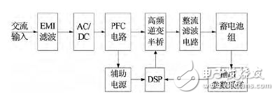
Figure 1 Block diagram of electric vehicle car charger
In view of the stringent requirements for volume and harmonics of pure electric vehicle chargers, this design uses Active Power Factor Correction (APFC) technology. The APFC has a variety of topologies. Since the boost topology has the advantages of simple drive circuit, high PF value, and special control chip, the main circuit of the Boost topology is selected. Considering various basic control methods, the average current control method with small harmonic distortion, insensitivity to noise and fixed switching frequency technology is selected.
This paper focuses on the design requirements of harmonic content, volume and anti-jamming performance for pure electric vehicle chargers with a power of 2 kW, focusing on PFC AC/DC converters, including system main circuit and control circuit design, and Based on the above research, the system simulation and experimental test verification research are carried out. The circuit diagram is shown in Figure 2.
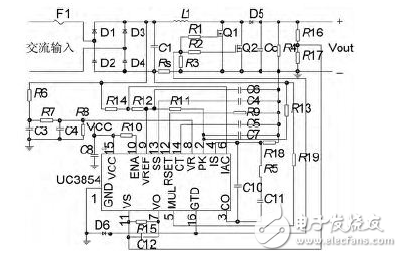
Figure 2 Boost PFC AC / DC converter circuit schematic
1 Boost PFC AC/DC converter
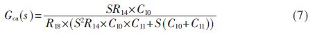
This paper focuses on the main circuit structure based on the Boost topology and the average current control strategy in continuous mode for the PFC AC/DC converter of the car charger with a power of 2 kW. The main circuit is composed of a rectifying circuit and a boost voltage boosting circuit; the control circuit adopts a double closed-loop control mode of a current inner loop and a voltage outer loop, and the principle block diagram is shown in FIG. 3 .
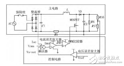
Figure 3 block diagram of the main circuit and control circuit
2 PFC AC / DC converter main circuit design
The main circuit of PFC AC/DC converter is composed of output filter capacitor, switching device, boost inductor and other components. The parameters are designed as follows.
2.1 Output Filter Capacitor
The output filter capacitor can filter the output voltage ripple caused by the switching action, and can maintain the output voltage within a certain range. The selected device needs to achieve the above two functions well.
2.1.1 Consider the output ripple voltage
![]()
Where: Co is the output filter capacitor, Pout is the output power of the main circuit, fin is the input voltage frequency of the grid, ΔVout is the peak-to-peak value of the output ripple voltage of the main circuit, and Vout is the output voltage of the main circuit.
2.1.2 Consider voltage maintenance time
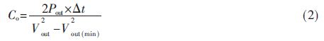
Where: Δt is the time when the output voltage of the main circuit drops from Vout to Vout(min).
According to the calculation results, three 220 μF/400 V and one 330 μF/400 V electrolytic capacitors are connected in parallel.
2.2 Switching device
The selection of power tube switching devices mainly considers the following parameters: withstand voltage value, on-state current value, and power tube switching frequency. In the case of high switching frequency, the MOS transistor is often selected, but the on-state current of a single MOS transistor is small. In order to increase the current carrying capacity, the system uses two MOS transistors in parallel. When the device is selected, the current flowing through the MOS transistor takes 2 times the margin, and the voltage across the MOS transistor takes 1.2 times the margin. In order to increase the flow capacity, two IPA60R165CP (650 V, 21 A) are connected in parallel.
2.3 boost inductor
The design idea of ​​the boost inductor is: first calculate the inductance, then select the appropriate core material, and finally combine the influence of the magnetic saturation on the inductance, and select the appropriate inductance and material.
The formula for calculating the inductance is:
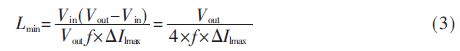
Where: Vin is the input voltage of the main circuit, f is the switching frequency, Lmin is the minimum value of the inductance, and ΔIlmax is the maximum value of the inductor current ripple. The minimum value of the boost inductor is determined to be 108 μH.
After determining the inductance, you need to select the appropriate core material. The boost inductor core materials of the APFC circuit include a magnetic powder core, a ferrite core, and a gap-free amorphous/microcrystalline alloy core. Based on the comprehensive analysis, considering the advantages of high magnetic flux density (BS), small volume and no air gap, the iron-silicon-aluminum magnetic powder core is selected as the core material.
When the main circuit current is large, the inductor will have a DC offset, resulting in saturation of the magnetic circuit. The larger the current, the greater the saturation of the magnetic circuit. Therefore, when selecting an inductor core, it is necessary to consider the problem of magnetic saturation. Considering comprehensively, the iron-silicon-aluminum core of model KS184060A is selected to be 60åŒ. When the saturation of the magnetic circuit is maximum, the inductance is still 110 μH, which is slightly larger than 108 μH.
3 PFC AC / DC converter control circuit design
The control circuit adopts a double closed-loop structure: the outer loop is a voltage loop, the inner loop is a current loop, and the current loop controls the input current tracking current of the main circuit to realize power factor correction. The output voltage of the voltage loop is compared with the output reference voltage through the voltage error amplifier, and the feedforward voltage and the input voltage are calculated by a multiplier to obtain an input reference current of the current loop. Through the adjustment of the current loop, the driving signal of the main circuit switch tube is turned on and off, the system power factor correction is realized, and the stable DC voltage is output. The role of the multiplier is mainly signal multiplication. Here, the focus of this paper is on the design of the voltage loop and current loop.
3.1 voltage loop design
One of the functions of the voltage loop is to feed back the change of the output voltage to the current loop; the second is to attenuate the second harmonic voltage to a specified level to reduce the distortion of the input current. In addition, due to the charging and discharging of the output capacitor, the output ripple voltage lags the input voltage. Therefore, the design of the voltage loop needs to consider sufficient phase shift to ensure that the output voltage ripple is in phase with the input voltage. In summary, it is necessary to set a reasonable compensation circuit so that the voltage loop can satisfy the above conditions.
When there is no compensation, the voltage loop open-loop transfer function expression is:
![]()
Where: Pin is the input power and ΔV is the voltage error amplifier output voltage range. The Bode diagram of the voltage open-loop transfer function is shown in the H curve in Fig. 4. The second harmonic is not attenuated, resulting in a large distortion of the input current. Therefore, it is necessary to set a pole to make the ripple voltage get better attenuation. At the same time, the ripple voltage is advanced by 90°.
The compensation circuit transfer function designed is:
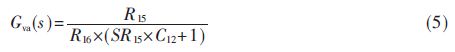
Considering comprehensively, the configuration pole frequency is equal to the crossing frequency. At this time, the phase margin is 45°, the system stability is good, and the second harmonic is greatly attenuated. The Bode diagram of the compensated voltage loop transfer function is shown in the N curve of Fig. 4, the second harmonic is greatly attenuated, and the ripple voltage is advanced by 90°.
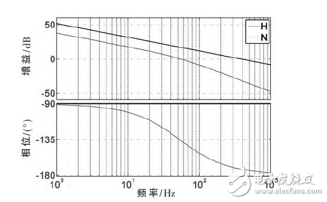
Figure 4: Bode diagram of the voltage loop transfer function before and after compensation
3.2 Current loop design
The function of the current loop is to adjust the input current of the main circuit to track the input voltage of the main circuit to achieve high PF control. The design idea of ​​the current loop is to increase the response speed through the reasonable design of the compensation circuit and ensure the stable operation of the system.
In the absence of a compensation circuit, the current loop consists of a PWM comparator and a power stage. The open-loop transfer function expression is:
![]()
The Bode diagram of the current open-loop transfer function is shown by the H curve in Figure 5. The current loop bandwidth is very narrow and the high-frequency noise is not well suppressed. To this end, the zero point is set by the low frequency to increase the low frequency gain and increase the bandwidth; at the same time, the pole is set at the high frequency to suppress the switching noise. The open loop transfer function of the designed compensation circuit is:
To this end, select the appropriate cutoff frequency, set the zero frequency and the pole frequency, so that the system's phase margin is above 45 °, while taking into account the current loop to meet the high gain and large bandwidth design requirements. Set the cutoff frequency to 6.65 kHz, the zero frequency is 4.5 kHz, the pole frequency is 46 kHz, and the phase margin is 48°. The Bode diagram of the current loop transfer function after adding the compensation circuit is shown in the N curve of Figure 5, adding compensation. After the current loop is at low frequency, the system bandwidth is large; at high frequencies, the switching noise is better attenuated; in addition, the system phase margin exceeds 45°, which can achieve stable operation of the system.
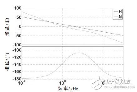
Figure 5: Bode diagram of the current loop transfer function before and after compensation
4 system simulation and experimental test
The system is simulated based on Saber simulation software. The main parameters of Boost PFC AC/DC converter are: inductance L=500 μH, output capacitance Co=990 μH, switching frequency fs=133 kHz, grid frequency fin=50 Hz, R16= 510 kΩ, R17=10 kΩ, R4=160 Ω, R5=0.01 Ω, other parameters are obtained through the aforementioned design flow. When the input voltage RMS values ​​are 140 V and 220 V, the system simulation and experimental tests are respectively performed. The simulation results are shown in Figure 6. The experimental test waveforms are shown in Figure 7.
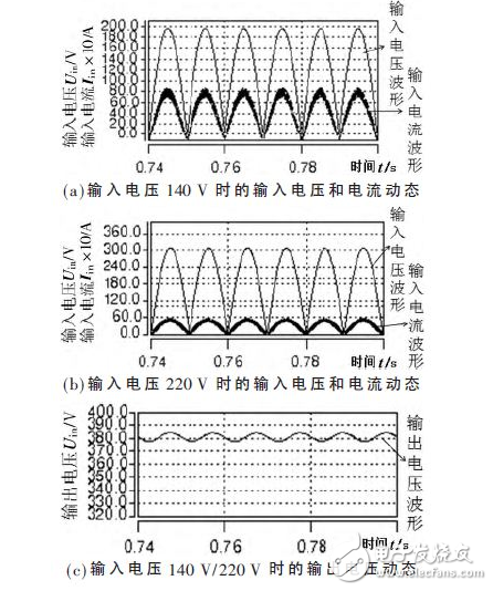
Figure 6 Input voltage, current and output voltage dynamics 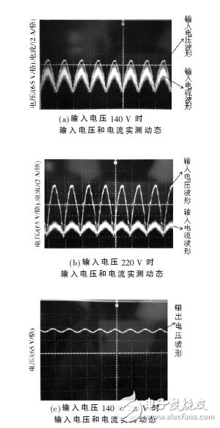
Figure 7 Boost PFC AC / DC converter measured dynamics
System simulation and experimental results show that the designed Boost PFC AC/DC converter can obtain stable DC output voltage over a wide input voltage range.
High Voltage Power Supply,High Voltage Lab Power Supply,High Voltage Dc Power Supply,High Voltage Ac Power Supply
Yangzhou IdealTek Electronics Co., Ltd. , https://www.idealtekpower.com