In the past 2016, in the computer industry, I believe that no concept is more popular than artificial intelligence. Entering 2017, experts say that the demand for artificial intelligence ecosystems will grow even more rapidly. Mainly focused on finding the "engine" that is more suitable for deep neural networks for performance and efficiency.
Today's deep learning systems rely on software-defined networks and the sheer computing power of big data learning to achieve their goals. Unfortunately, this type of computing configuration is difficult to embed in systems where computing power, storage size, and bandwidth are limited (such as cars, drones, and IoT devices).
This presents a new challenge for the industry, how to embed the computing power of deep neural networks into terminal devices through innovation.
Movidius CEO Remi El-Ouazzane said a few months ago that placing artificial intelligence on the edge of the network would be a big trend.

Remi El-Ouazzane
When asked why artificial intelligence was “rushed†to the edge of the network, CEA Architecture Fellow Marc Duranton gave three reasons: security, privacy, and economy. He believes that these three points are important factors driving the industry to process data at the terminal. He pointed out that in the future, there will be more demand for “transforming data into informationâ€. And the sooner these data are processed, the better, he added.

CEA Architecture Fellow Marc Duranton
Camera, if your driverless car is safe, then these unmanned functions do not need to rely on the alliance for a long time; if the old man falls at home, then this situation should be detected and judged on the spot. These are very important for privacy reasons, Duranton stressed.
But this does not mean that all the pictures of the ten cameras in the home are collected and sent to me, which is called a reminder of a number. This does not reduce "energy, cost and data size," Duranton added.
The competition officially opened
From the current situation, chip suppliers have realized the growing demand for inference engines. Many semiconductor companies, including Movidus (Myriad 2), Mobileye (EyeQ 4 & 5) and Nvidia (Drive PX), are competing for low-power, high-performance hardware accelerators. Help developers better perform "learning" in embedded systems.
From the perspective of the actions of these vendors and the development direction of SoC, in the post-smartphone era, the inference engine has gradually become the next target market pursued by semiconductor manufacturers.
Earlier this year, Google's TPU turned out to be an indication of the industry's intention to drive innovation in machine learning chips. When the chip was released, the search giant said that the performance per watt of TPU would be an order of magnitude higher than that of traditional FPGAs and GPUs. Google also said that the accelerator has also been applied to the AlphaGo system, which was popular around the world earlier this year.
But since its release, Google has never disclosed the specifics of TPU, let alone sell it.
Many SoC practitioners have come to the conclusion from Google's TPU that they believe that machine learning requires a customized architecture. But when they do chip design for machine learning, they are doubtful and curious about the architecture of the chip. At the same time, they want to know if the industry already has a tool to measure the performance of deep neural networks (DNN) in different forms.
Tools have arrived
CEA claims that they have prepared for the inference engine to explore different hardware architectures, and they have developed a software architecture called N2D2. They are enough to help designers explore and claim the DNN architecture. "We developed this tool to help DNN choose the right hardware," Duranton said. By the first quarter of 2017, this N2D2 will be open source. Duranton promised.
N2D2 is characterized by not only comparing hardware based on recognition accuracy, but also comparing it in terms of processing time, hardware cost and energy loss. Because the hardware configuration parameters required for different deep learning applications are different, so the above points are the most important, Duranton said.
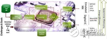
How N2D2 works
N2D2 provides a reference standard for existing CPUs, GPUs, and FPGAs.
Barriers to edge computing
As a senior research organization, CEA has conducted in-depth research on how to extend DNN to the field of edge computing. When asked about the obstacles to this kind of advancement, Duranton pointed out that these "floating point" server solutions cannot be applied due to power consumption, size and latency limitations. This is the biggest obstacle. Other obstacles include "a large number of Macs, bandwidth and size on the chip," Duranton added.
That is to say how to integrate this "floating point" method is the first problem that should be solved.
Duranton believes that some new architectures are inevitable, and some new coding like "spike code" is inevitable.
According to CEA research, even binary encoding is not required. They believe that time coding like spike coding can emit more powerful energy at the edge.
Spike coding is popular because it clearly demonstrates the decoding of data within the nervous system. In the deepest sense, these event-based encodings are compatible with dedicated sensors and pre-processing.
This extremely similar encoding to the nervous system makes hybrid analog and digital signals easier to implement, which also helps researchers create low-power hardware accelerators.
CEA is also thinking about the potential to adjust the neural network architecture to edge computing. Duranton pointed out that people are now pushing to use 'SqueezeNet to replace AlexNet. According to reports, in order to achieve the same accuracy, the former uses 50 times less parameters than the latter. This type of simple configuration is important for edge computing, topology, and reducing the number of Macs.
Duranton believes that moving from a classic DNN to an embedded network is a spontaneous act.
P-Neuro, a temporary chip
CEA's ambition is to develop a neuromorphic circuit. Researchers believe that such a chip is an effective complement to push data extraction on the sensor side in deep learning.
But before reaching this goal, CEA got along with a lot of expediency. For example, the development of tools such as D2N2 helps chip developers develop high-TOPS DNN solutions.
For those who want to transfer DNN to edge computing, they also have the corresponding hardware to implement. This is the low-power programmable accelerator from CEA, P-Neuro. The current P-Neuro chip is based on FPGA development. But Duranton said they have turned this FPAG into an ASIC.

P-Neuro demo compared to embedded CPU
In CEA's lab, Duranton has built a facial recognition convolutional neural network (CNN) in this FPAG-based P-Neuro. This P-Neuro-based demo is compared to the embedded CPU. (Raspberry pie, Android device with Samsung Exynos processor). They also all run the same CNN application. They all arranged to perform "face feature extraction" from a database of 18,000 images.
According to the example, the speed of P-Neuro is 6,942 images per second, while the power consumption is only 2,776 images per watt.
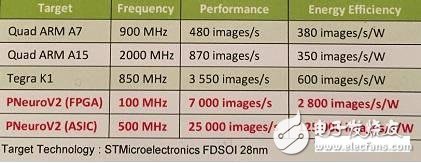
P-Neuro and GPU, CPU comparison
As shown, the FPGA-based P-Neuro works faster and consumes less power at 100Mhz operating frequency than the Tegra K1.
P-Neuro is built on a cluster-based SIMD architecture that is well known for its optimized hierarchical memory architecture and internal connectivity.
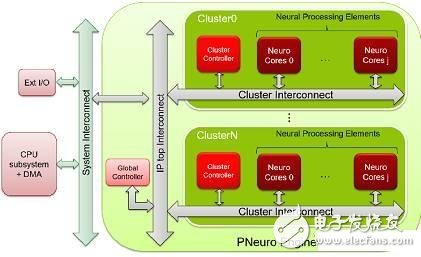
Block diagram of P-Neuro
For CEA researchers, P-Neuro is only a short-term solution. The current P-Neuro is built on a CMOS device using binary encoding. Their team is building a full CMOS solution and is planning to use spike coding.
In order to take full advantage of the advantages of advanced equipment and break the issue of density and power, their team set a higher goal. They considered RRAM as a synapse element and considered processes such as FDSOI and nanowires.
In a "EU Horizon 2020" program, they hope to make a neuromorphic architecture chip that can support the most advanced machine learning. It is also a spike-based learning mechanism.
Neuromorphic processor
This is a project called NeuRAM3. By then, their chips will have ultra-low power, size and highly configurable neural architecture. Their goal is to create a product that can reduce power consumption by a factor of 50 compared to traditional solutions.
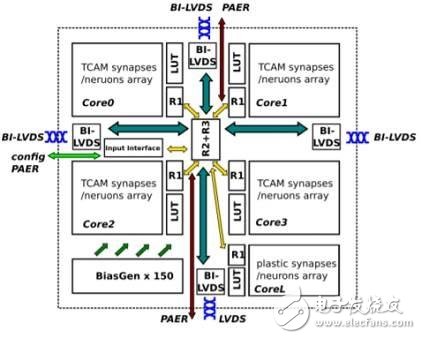
Neuromorphic processor
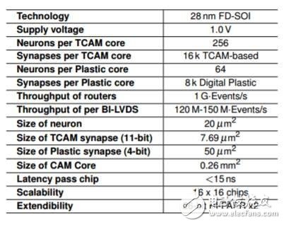
Basic parameters of the Neuromorphic processor
According to reports, this solution includes the integrated 3D technology based on the FD-SOI process, and also uses RRAM to make synaptic elements. Under the NeuRAM3 project, this new mixed-signal multi-core neuromorphic chip device can significantly reduce power consumption compared to IBM's TrueNorth.
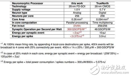
Contrast with IBM's TrueNorth
Participants in the NeuRAM3 project include IMEC, IBM Zurich, ST Microelectronics, CNR (The NaTIonal Research Council in Italy), IMSE (El InsTItuto de Microelectrónica de Sevilla in Spain), the University of Zurich and the University of Jacobs in Germany.
More AI chip competition
In fact, the AI ​​chip market has attracted a lot of players, both traditional semiconductor manufacturers and so-called start-ups, have begun to go to this next gold mine. In addition to the CEA mentioned above. Let's take a look at what other AI chips are on the market.
First, the follow-up of traditional manufacturers
(1) Nvidia
NVIDIA is the GPU overlord. Although they missed the mobile era, they seem to have regained their glory in the AI ​​era. From the stock trend in the past year, they can see the confidence of the market. Let's see what plans he has in this area.
In April of this year, Nvidia released an advanced machine learning chip, the Tesla P100 GPU. According to Nvidia CEO Huang Renxun, this product has 12 times faster processing speed than NVIDIA's predecessor. The $2 billion developed chip integrates 150 billion transistors.
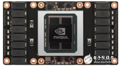
According to the introduction, the new NVIDIA Pascal? The architecture enables the Tesla P100 to deliver exceptional performance for HPC and very large workloads. With more than 20 trillion FP16 floating-point performance per second, the optimized Pascal brings exciting new possibilities for deep learning applications.
By adding CoWoS (wafer-based chip) technology using HBM2, the Tesla P100 tightly integrates computing and data in the same package with more than three times the memory performance of previous generation solutions. This allows the problem-solving time of data-intensive applications to leapfrog across the ages.
Furthermore, because of the NVIDIA NVLink? Technology, the fast nodes of the Tesla P100 can significantly reduce the time it takes to provide solutions for applications with strong scalability. Server nodes with NVLink technology can interconnect up to eight Tesla P100s with 5x PCIe bandwidth. This design is designed to help solve the globally significant challenges of HPC and deep learning with significant computing needs.
(2) Intel
In November of this year. Intel has released an AI processor called Nervana, which they claim will test the prototype in the middle of next year. If all goes well, the final form of the Nervana chip will be available in 2017. The chip is based on a company called Nervana that Intel bought earlier. According to Intel, the company is the first company on the planet to build chips for AI.
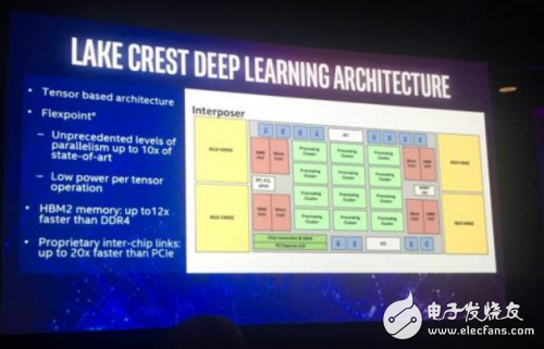
Intel disclosed some details about the chip. According to them, the project code is "Lake Crest" and will use Nervana Engine and Neon DNN related software. . The chip accelerates a variety of neural networks, such as the Google TensorFlow framework. The chip consists of a so-called "processing cluster" array that handles simplified mathematical operations called "active points." This method requires less data than floating-point operations, resulting in a 10x performance boost.
Lake Crest uses private data connections to create larger, faster clusters with a circular or other topology. This helps users create larger, more diverse neural network models. This data connection contains 12 100Gbps bidirectional connections, and its physical layer is based on 28G serial-to-parallel conversion.
The 2.5D chip is equipped with 32GB of HBM2 memory and has a memory bandwidth of 8Tbps. There is no cache in the chip, and the software is used to manage on-chip storage.
Intel did not disclose the future roadmap for this product, only that it plans to release a version called Knights Crest. This version will integrate future Xeon processors and Nervana acceleration processors. This is expected to support the Nervana cluster. However, Intel did not disclose how and when these two types of chips will be integrated.
As for the integrated version, there will be more performance and easier programming. Current graphics processing chip (GPU)-based accelerated processors make programming more complicated because developers maintain separate GPU and CPU memory.
According to reports, by 2020, Intel will launch chips to improve the performance of neural network training by 100 times. One analyst said the goal was "extremely radical." There is no doubt that Intel will quickly move this architecture to more advanced manufacturing processes, competing with GPUs that already use 14nm or 16nm FinFET processes.
(3) IBM
Centennial giant IBM, who published wtson a long time ago, has now invested in a lot of research and development. In the past year, he also couldn't help but invest in the research and development of human brain chips. That is TrueNorth.
TrueNorth is the latest achievement of IBM's participation in DARPA's research project, SyNapse. SyNapse's full name is Systems of Neuromorphic AdapTIve PlasTIc Scalable Electronics, and SyNapse is synaptic. The ultimate goal is to develop a broken von? The hardware of the Neumann system.
This chip treats the digital processor as a neuron and uses memory as a synapse. Unlike traditional von Neumann architecture, its memory, CPU and communication components are fully integrated. Therefore, the processing of information is completely local, and since the amount of data processed locally is not large, the bottleneck between the traditional computer memory and the CPU no longer exists. At the same time, neurons can communicate with each other conveniently and quickly. As long as they receive pulses (action potentials) from other neurons, these neurons will act simultaneously.
In 2011, IBM first introduced a single-core chip prototype with 256 neurons, 256 × 256 synapses and 256 axons. The prototype at the time was already able to handle complex tasks like playing Pong games. However, it is relatively simple. In terms of scale, such a single-core brain capacity is only equivalent to the level of the brain.
However, after three years of hard work, IBM finally made a breakthrough in complexity and usability. 4096 cores, 1 million "neurons", 256 million "synapses" are integrated between a few centimeters in diameter (1/16 of the prototype size in 2011), and consume less than 70 Milliwatts, IBM's integration is really impressive.
What can such a chip do? The IBM research team has used the NeoVision2 Tower dataset that has been done with DARPA for demonstrations. It can identify people, bicycles, buses, trucks, etc. in the crossroads video of Stanford University's Hoover Tower at a normal speed of 30 frames per second, with an accuracy rate of 80%. In contrast, a notebook programming is 100 times slower to complete the same task, and the energy consumption is 10,000 times that of the IBM chip.
As with traditional computers using FLOPS (floating operations per second) to measure computing power, IBM uses SOP (synaptic operations per second) to measure the power and energy efficiency of such computers. The energy required to complete the 46 billion SOP is only 1 watt—as described at the beginning of the article, this capability is a supercomputer, but a small hearing aid battery can be driven.
The communication efficiency is extremely high, which greatly reduces energy consumption. This is the biggest selling point of this chip. Each core of TrueNorth has 256 neurons, each of which is connected to 256 neurons inside and outside.
(4) Google
In fact, on Google, I am very entangled, whether this is a new force, or a traditional company. But considering Google has been for so many years, I will put him in the tradition. Although the tradition is also very new. And Google's artificial intelligence related chip is the TPU. That is the Tensor Processing Unit.
The TPU is a dedicated chip designed specifically for machine learning applications. By reducing the computational accuracy of the chip and reducing the number of transistors required to implement each computational operation, the number of operations per second of the chip can be increased, so that a fine-tuned machine learning model can be run on the chip. Faster, and thus faster, for users to get smarter results. Google embeds the TPU accelerator chip into the board and uses the existing hard disk PCI-E interface to access the data center server.
According to Urs Holzle, senior vice president of Google, the current use of Google TPU and GPU will continue for a while, but it is also said that the GPU is too general and Google prefers chips designed for machine learning. The GPU can perform drawing operations and has many uses. The TPU is an ASIC, which is a special specification logic IC designed for specific purposes. Because it only performs a single job, it is faster, but the disadvantage is higher cost. As for the CPU, Holzle said that the TPU will not replace the CPU, and the TPU is only developed to deal with unresolved issues. But he also pointed out that he hopes that the chip market will have more competition.
If the AI ​​algorithm changes (logically the algorithm should change over time), do you want a chip that can be reprogrammed to accommodate these changes? If this is the case, another chip is suitable, it is the FPGA (Field Programmable Gate Array). FPGAs can be programmed to be different from ASICs. Microsoft uses some FPGA chips to enhance the AI ​​capabilities of Bing search engines. We naturally ask: Why not use an FPGA?
CD Car Phone Holder,Car CD Slot Mount Holder,Car Phone Mount Holder,Car Accessory CD Phone Holder
Ningbo Luke Automotive Supplies Ltd. , https://www.nbluke.com