The amplifier introduced in this article takes Sony's C1891A as the core and LM1875 as the main power amplifier. It has the characteristics of low price, simple and easy production, and obvious effects. It is very suitable for beginners to make their own.
Circuit principle:
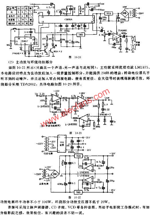
1. Surround sound processing part
C1891A is a home theater 4D surround sound processing circuit launched by Sony Corporation of Japan. This circuit uses a matrix phase-shifting surround sound amplifier. Three sound field effect modes including concert hall, movie theater, and analog stereo are also specially established. The specific application circuit is shown in Figure 10-20. The brief introduction of each function pin is as follows: pins 2 and 3 are left and right channel outputs; pins 8 and 9 are left and right channel inputs, and pin 10 is surround output; 11. Pin 12 is the state selection pin (connecting + 5V level can change the sound field mode), using the integrated circuit CD4017 to make a one-button state selection switch, with color light indication, and the effect is good; Pin 13 is the effect adjustment terminal.
The products can provide various specifications of rectifier bridge devices according to customer requirements. The electrical properties, appearance, reliability, safety indicators and environmental protection indicators of the products all meet the relevant standards.
Planar Die Construction Sealed Glass Case Ideally Suited for Automated Insertion - 75V Nominal Zener Voltages
Case: MiniMELF, Glass Terminals: Solderable per MIL-STD-202, Method 208 Polarity: Cathode Band Approx. Weight: 0.05 grams= 25°C unless otherwise specified Symbol Pd VF RqJA Tj, TSTG Value to +175 Unit mW V K/W °C
Characteristic Forward Voltage = 200mA Thermal Resistance, Junction to Ambient Air (Note 2) Operating and Storage Temperature Range Notes:
1. Tested with Pulses, 20ms. 2. Valid provided that Electrodes are kept at Ambient Temperature.
1. Tested with pulses = 20 ms. 2. Valid provided that electrodes are kept at ambient temperature.
VZ, ZENER VOLTAGE (V) Fig. 1, Zener Current vs Zener Voltage
25 20 VZ, ZENER VOLTAGE (V) Fig. 8, Zener Current vs Zener Voltage
TA, AMBIENT TEMPERATURE (°C) Fig. 3, Power Dissipation vs Ambient Temperature
15 20 VZ, ZENER VOLTAGE (V) Fig. 4, Differential Zener Impedance
VZ, ZENER VOLTAGE (V) Fig. 5, Junction Capacitance vs Zener Voltage
MINI MELF,Smd mini melf,zener mini melf,mini melf package,mini melf resistor,mini melf diode,mini melf resistor datasheet
Changzhou Changyuan Electronic Co., Ltd. , https://www.changyuanelectronic.com