MCS-51 interrupt related registers, interrupt entry address and number explain
The MCS-51 microcontroller is an integrated circuit chip. It is a CPU with a data processing capability using a VLSI technology. It has a CPU random access memory RAM, a read-only memory ROM, a variety of I/O ports and an interrupt system, and a timer. / Functions such as timers (which may also include display driver circuits, pulse width modulation circuits, analog multiplexers, A/D converters, etc.) are integrated into a small, complete computer system built on silicon. This article details the MCS-51 and interrupt related registers, interrupt entry address and number, specific follow Xiaobian together to find out.
MCS-51 microcontroller pin diagram and function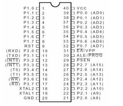
1, power supply
Vcc: chip power supply, typically +5V;
Vss: ground.
2, the clock
XTAL1 and XTAL2: Inverting input and output of crystal oscillator circuit. When using the internal oscillator circuit, an external crystal oscillator is required. Commonly used are 4M, 6M, 11.0592M, and 12M. When the external oscillation input is used, XTAL1 is grounded and XTAL2 is connected to the external oscillation pulse input.
3, control line
The MCS-51 microcontroller has a total of four control lines, of which three are multiplex lines and have two functions.
(1) ALE/PROG: Address latch enable/program pulse.
ALE: ALE function in normal use, mainly used to latch the 8-bit address sent by port P0. The P0 port generally transmits the lower 8-bit address and data signals in a time-divisional manner, and both are binary numbers. To distinguish whether it is a low 8-bit data signal or an address signal, see the ALE pin. When the ALE signal is valid, the P0 port transmits the lower 8-bit address signal; when the ALE is invalid, the P0 port transmits 8-bit data signals. Generally, the content transmitted on the P0 port is locked at the falling edge of the ALE pin, that is, the lower 8-bit address signal.
When the CPU does not execute the instruction to access the external RAM (MOVX), ALE outputs at a fixed frequency of 1/6 of the clock oscillation frequency, so the ALE signal can also be used as an external chip clock signal. However, when the CPU performs an access to external RAM (MOVX), ALE will skip an ALE pulse.
PROG: When the microcontroller is programming, this pin is input with a programming pulse (provided by the programmer).
(2) PSEN: External ROM read strobe signal.
When the microcontroller reads the external ROM, PSEN is output twice in each machine cycle. PSEN is equivalent to the strobe signal allowed by the output of the external ROM chip. However, it is invalid when reading on-chip ROM and reading off-chip RAM.
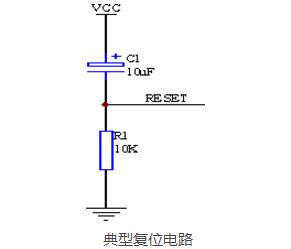
(3) RST: Reset pin.
RST is the power on reset input end of the one-chip computer, if keep the high level above two machine cycles continuously on this pin, the one-chip computer can realize reset operation, after resetting the procedure begins to carry out from 0000H. In general applications, the RC circuit can be used to implement the power-on reset of the microcontroller. In some industrial control applications such as high demand applications, a dedicated watchdog chip is generally used for reset and power supply monitoring. A typical RC power-on reset circuit is shown in the figure. Show:
(4) EA/VPP: Internal/external ROM select/EPROM programming power supply.
EA: During normal operation, the EA is the inside and outside ROM selection. The addressing range of MCS-51 type single-chip microcomputer is 64KB, 4K on-chip, 60K off-chip. When EA is high, the on-chip ROM is accessed first. When the program length exceeds 4K, it will automatically turn to execute the external ROM. program. When the EA is low, the microcontroller only accesses the external ROM. For the old 8031 ​​MCU (without ROM in the chip), the EA must be grounded. Most of the current microcontrollers have their own ROM, so the general application will also connect EA high.
VPP: For microcontrollers with internal EPROM, this pin is used to apply programming power during on-chip EPROM programming.
4, I/O pin
The MCS-51 microcontroller has four 8-bit parallel I/O ports, a total of 32 programmable I/O pins. Each of the four I/O ports has its own function. Under normal circumstances, P0 is dedicated to time-divided transmission of low-order 8-bit address signals and 8-bit data signals. P2 port is dedicated to the transmission of high-order 8-bit address signals. P3 port is used most of the time. Used for the second function. Of course, all I/O ports can be used as ordinary input/output ports.
MCS-51 interrupt related register, interrupt entry address and numberFirst, interrupt entry address and number
The MCS-51 checks each interrupt source sequentially at every machine cycle, processing all activated interrupt requests at priority in the S6 of the machine cycle. At this time, if the CPU is not processing higher or same priority interrupts, or The machine cycle is not the last machine cycle of the instruction being executed, or the CPU is not executing the RETI instruction or accessing the IE and IP instructions (because the MCS-51 interrupt system features specified, after the execution of these instructions, but also to continue Only one instruction is executed to respond to the interrupt. The CPU responds to the most advanced interrupt request activated on the next machine cycle.
The main content of the interrupt response is that the hardware automatically generates a long call to the LCALL addr16 instruction, where addr16 is the corresponding interrupt area entry address in the program memory. The service program entry addresses for these interrupt sources are as follows:
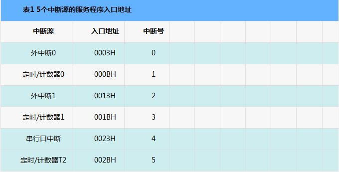
After generating the LCALL instruction, the CPU executes it immediately. First, the contents of the PC (program counter) are pushed into the stack protection breakpoint, and then the interrupt entry address is given to the PC, and the CPU executes the program with the new PC address (ie, the interrupt service program entry address).
It is worth mentioning that there are only 8 units in each interrupt area. Under normal circumstances (unless the interrupt program is very simple), it is impossible to install the next complete interrupt service program. Therefore, an unconditional branch instruction is usually placed in these entry address areas so that the program can execute a real interrupt service program according to the actual address transferred.
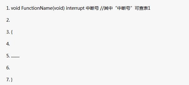
For assembly, the general form of the interrupt function is:

For C language, the general form of the interrupt function is:
Second, the interrupt-related registers
1, the timer control register TCON
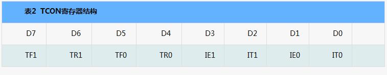
IE1: The external edge triggers the interrupt 1 request flag and its function and operation are similar to TF0.
IT1: External interrupt 1 type control bit, set or cleared by software, is used to control the type of trigger signal for external interrupts. IT1=1, edge trigger. IT=0 is a level trigger.
IE0: The external edge triggers the interrupt 0 request flag. Its function and operation are similar to those of IE1.
IT0: External interrupt 0 type control bit, set or cleared by software, is used to control the trigger signal type of the external interrupt. Its function and operation are similar to IE1.
2. Interrupt enable register IE
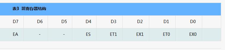
EA: interrupt total control bit, EA=1, CPU open interrupt. EA=0, CPU disables all interrupts.
ES: Serial port interrupt control bit, ES=1 allows serial port interrupt, ES=0, shields serial port interrupt.
ET1: Timer/Event Counter T1 interrupt control bit. ET1=1, allowing T1 interrupt, ET1=0, disable T1 interrupt.
EX1: External interrupt 1 interrupt control bit, EX1 = 1, allows external interrupt 1 interrupt, EX1 = 0, disable external interrupt 1 interrupt.
ET0: Timer/Event Counter T0 interrupt control bit. ET1=1, allow T0 interrupt, ET1=0, disable T0 interrupt.
EX0: External interrupt 0 interrupt control bit, EX1 = 1, which allows external interrupt 0 interrupt, EX1 = 0, disable external interrupt 0 interrupt.
3, interrupt priority control register IP
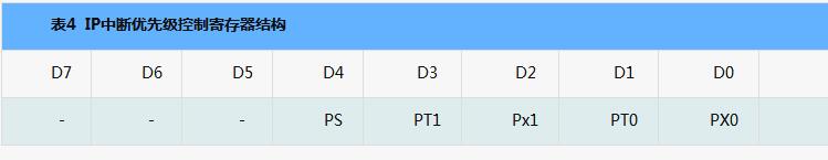
PS: Serial port interrupt port priority control bit, PS=1, serial port interrupt is declared as high priority interrupt, PS=0, serial port is defined as low priority interrupt.
PT1: Timer 1 priority control bit. PT1 = 1, declares Timer 1 as a high priority interrupt, and PT1 = 0 defines Timer 1 as a low priority interrupt.
PX1: External interrupt 1 priority control bit. PT1=1, declare external interrupt 1 as high priority interrupt, PX1=0 define external interrupt 1 as low priority interrupt.
PT0: Timer 0 priority control bit. PT1=1, declare timer 0 as high priority interrupt, PT1=0 define timer 0 as low priority interrupt.
PX0: External interrupt 0 priority control bit. PT1=1, declare external interrupt 0 as high priority interrupt, PX1=0 define external interrupt 0 as low priority interrupt.
4, serial communication control register SCON
It is an addressable special register for serial data communication control. The unit address is 98H. Its structure is as follows:
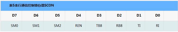
TI: Send interrupt flag.
In mode 0, after the 8th bit data is transmitted, it is set by hardware. In other modes, it is set by hardware before the transmit or stop bit. Therefore, TI=1 indicates that the frame transmission ends and TI can be cleared by software.
RI: Receive interrupt flag.
After receiving the 8th bit data, this bit is set by hardware. In other working modes, this bit is set by hardware. RI=1 indicates that the frame reception is completed.
5, T2 state control register T2CON
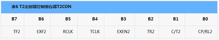
TF2: T2 overflow interrupt flag. TF2 must be cleared by user program "0". When T2 is used as a serial baud rate generator, TF2 will not be set to "1".
EXF2: Timer T2 external interrupt flag. When EXEN2 is 1, the interrupt flag DXF2 is set when a negative transition occurs in T2EX (P1.1), and EXF2 must be cleared by the user program to “0â€.
EXEN2: T2 External Interrupt Allowance Flag
Easy Electronic Technology Co.,Ltd , https://www.pcelectronicgroup.com