In the past one or two years, driven by Apple's iPhone, the smartphone market has expanded rapidly. An important feature of portable products such as smartphones is the increasing functionality to support a wider range of consumer needs. However, the operating voltages of integrated circuits (ICs) or modules used to support different functions inside portable products such as smart phones are often different. For example, the baseband processor and application processor voltages are generally between 1.5 V and 1.8 V, and many existing ones are available. The operating voltage is generally 2.6 to 3.3 V. For example, the USIM card, Wi-Fi module, and FM tuner module operate at 2.8 V, while the camera module is 2.7 V.
This article refers to the address: http://

Therefore, there is an input/output voltage mismatch between different ICs and peripheral modules in portable products such as smart phones. In order for these devices to communicate with each other, efficient logic voltage level conversion is required. The so-called logic level converters are ICs and modules or printed circuit boards (PCBs) that connect different operating voltages to provide a system integration solution.
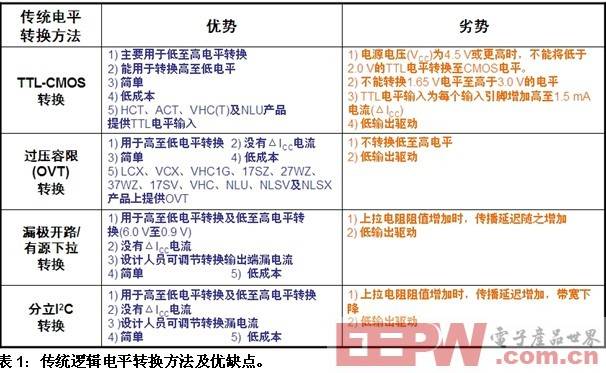
Traditional logic level conversion method and its advantages and disadvantages
Since transistor-transistor logic (TTL) and complementary metal-oxide-semiconductor (CMOS) are standard levels in logic circuits, TTL-CMOS input conversion is common in traditional logic level shifting methods. This conversion method is simple and low in cost, and is mainly used for low-to-high level conversion, and can also be used to convert high level to low level. This conversion method also has some disadvantages. Other traditional logic level conversion methods include overvoltage tolerance (OVT) voltage conversion, open-drain (OD)/active pull-down conversion, and discrete I2C conversion, each with its own advantages and disadvantages. See Table 1.
Dual power logic level conversion and application
Power is consumed in logic level shifting. For example, in a low-to-high transition, in order to output a high logic level, the input voltage (Vin) is lower than VCC, and the power supply current variation (ΔICC) is always higher, so the power consumption is also higher. In order to solve the problem of high power consumption, dual supply voltage (VCCA and VCCB) logic level converters can be used. When the logic supply voltage (VL) is equal to Vin, ΔICC is 0, thereby reducing power consumption.
Common dual-supply logic level shifting includes unidirectional conversion, bidirectional conversion with directional control pins, auto-sensing bidirectional conversion (push-pull output), and automatic sensing bi-directional conversion for open-drain applications such as I2C The structure diagram is shown in Figure 2.
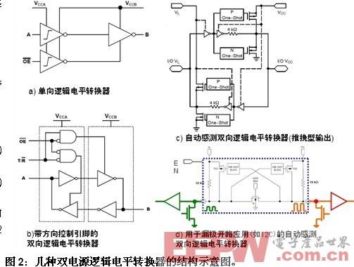
In these dual-supply logic level shifting methods, the principle of unidirectional logic level shifting is in the output enable (Output Enable, ![]() When it is low, it provides A point to B point conversion; when the output is enabled high level, A and B show high resistance state (Hi-Z), which is usually treated as resistance infinity, which is equivalent to no connection. through. Common dual-supply unidirectional logic level shifters are such as ON Semiconductor's NLSV1T34AMX1TCG, NLSV2T244MUTAG, NLSV4T3234FCT1G, NLSV8T244MUTAG, NLSV22T244MUTAG, and so on. Applications for these dual-supply unidirectional logic level shifters include general purpose input and output (GPIO) ports, serial peripheral interface (SPI) ports, and universal serial bus (USB) ports.
When it is low, it provides A point to B point conversion; when the output is enabled high level, A and B show high resistance state (Hi-Z), which is usually treated as resistance infinity, which is equivalent to no connection. through. Common dual-supply unidirectional logic level shifters are such as ON Semiconductor's NLSV1T34AMX1TCG, NLSV2T244MUTAG, NLSV4T3234FCT1G, NLSV8T244MUTAG, NLSV22T244MUTAG, and so on. Applications for these dual-supply unidirectional logic level shifters include general purpose input and output (GPIO) ports, serial peripheral interface (SPI) ports, and universal serial bus (USB) ports.
The bidirectional logic level shifter with directional control pins works as follows: ![]() Pin and direction control (DIRection, T/
Pin and direction control (DIRection, T/ ![]() When the pin is low, provide B point to point A conversion;
When the pin is low, provide B point to point A conversion; ![]() Pin is low, T/
Pin is low, T/ ![]() When the pin is high, provide point A to point B conversion;
When the pin is high, provide point A to point B conversion; ![]() When the pin is high, the direction from point A to point B and from point B to point A are in a high impedance state, which is equivalent to not being turned on. ON Semiconductor is about to introduce a bidirectional logic level shifter with directional control pins. A common application for such converters is memory and I/O devices that are accessed in bytes.
When the pin is high, the direction from point A to point B and from point B to point A are in a high impedance state, which is equivalent to not being turned on. ON Semiconductor is about to introduce a bidirectional logic level shifter with directional control pins. A common application for such converters is memory and I/O devices that are accessed in bytes.
The automatic sensing bidirectional logic level shifter (push-pull output) works by setting the enable (EN) pin low when the converter is in standby; the EN pin is high, I/O level When the constant is unchanged, the converter is in steady state; when the EN pin is high and the I/O level changes, the converter detects the change and generates a pulse, and the I/O is pulled up by the P-channel MOSFET (PMOS) to Faster. Typical auto-sensing direction bidirectional logic level shifters (push-pull outputs) are such as ON Semiconductor's NLSX3012MUTAG, NLSX3013FCT1G, NLSX3013BFCT1G, NLSX4014MUTAG, and NLSX3018MUTAG. Common applications for such converters include Universal Asynchronous Receiver Transmitter (UART), USB ports, 4-wire SPI ports, and 3-wire SPI ports.
The auto-sensing bidirectional logic level shifter for open-drain applications (such as I2C) also contains three states: the EN pin is high, the NMOS is on, it is active, and the input I/O level Pull down to ground, that is, input low level; EN pin is high level, NMOS is in high impedance state, it is in working state, output I/O level is pulled up to VCC, ie input high level; EN pin When low, the converter is in standby. Typical automatic sensing bidirectional logic level shifters for open-drain applications such as I2C are such as ON Semiconductor's NLSX4373MUTAG, NLSX4348FCT1G, and NSLX4378BFCT1G. Common applications for such converters include the I2C bus, Subscriber Identity Module (SIM) card, single-wire (1-Wire) bus, display module, Secure Digital Input Output (SDIO) card, and more.
Among the above-mentioned dual-supply logic level shifters, the automatic sensing converter without the direction control pin and the converter with the direction control pin have their advantages and disadvantages. The advantages of the auto-sensing converter are mainly to minimize the I/O line of the microcontroller. It is a simple solution for asynchronous communication. The disadvantage is that the cost is higher than the converter with lower bandwidth than the control pin with direction. . The converter with directional control pins has the advantage of being a commodity component with low cost and is a simple solution for memory-mapped I/O. The disadvantage is the large number of microcontroller pins.
In automatic sensing converters without directional control pins, there are also differences between integrated solutions (such as NLSX3373) and discrete solutions (such as NTZD3154N). The integrated solution NLSX3373 is a single IC, which is estimated to occupy only 2.6 mm2 of printed circuit board (PCB) space. The discrete solution NTZD3154N uses dual MOSFETs and four 01005 packages (ie 0402) resistors. The estimated total PCB space is 3.3. Mm2. The integrated solution provides a low-power standby mode, while the discrete solution does not provide a high-impedance/standby mode. The low voltage operating characteristics, bandwidth and circuit characteristics of the two different solutions are also different.
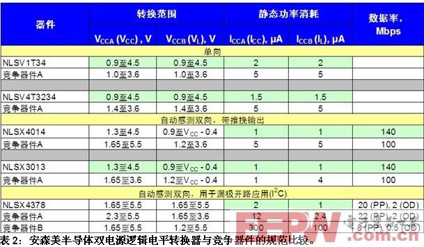
ON Semiconductor Dual Power Level Translator Specifications and Requirements
ON Semiconductor's dual-supply logic-level converters offer many advantages over competing devices. These advantages include a wider voltage conversion range, lower static power consumption, and/or support for higher data rates. For example, the dual-supply conversion range of ON Semiconductor's NLSX3013 with push-pull output is 1.3 V to 4.5 V and 0.9 V to VCC – 0.4 V, respectively, and the competing devices with close performance are 1.65 V to 3.6 V and 1.2 V to VCC – 0.4 V; both support data rates of 140 Mbps and 100 Mbps, respectively. See Table 2 for a more specific comparison.
ON Semiconductor's automatic sensing bidirectional converters with push-pull outputs, such as the NLSX4014, have their input drive current requirements. Assume that the I/O power supply voltage VL (point A) = 0 V, and to be positively converted to 2.8 V (that is, from low level to high level), initially point A = point B = 0 V, IIN1 flows into the CMOS device. Therefore, IIN » IIN2, peak current IIN » 2.8 V / 1 kΩ = 2.8 mA. This converter is designed to drive CMOS inputs and should not use resistive pull-up or pull-down loads with resistances below 50 kΩ (see Figure 3). In addition, in large capacitive loads, push-pull type auto-sensing bidirectional converters should not be used, otherwise the output distortion will be large, and a switch type level shifter should be used.

In addition, ON Semiconductor's dual-supply level shifters are available in small, rugged packages such as ULLGA6, UDFN6, UDFN8, UQFN12, UDFN20, uBump11, uBump12, and uBump20, where the UDFN6 package measures only 1.2 mm by 1.0 mm. The uBump12 package measures only 1.54 mm x 2.02 mm. These compact and rugged packages are ideal for portable applications such as smartphones.
ON Semiconductor's complete lineup of logic level shifters
As the world's leading supplier of high-performance, energy-efficient silicon solutions, ON Semiconductor has introduced a complete array of excellent logic level conversion solutions, such as dual power converters, MiniGateTM series switches with OVT, and MiniGateTM bus switches.
Among them, dual supply voltage logic level shifters support a wide range of high to low and low to high level conversion, and support unidirectional and bidirectional signal flow, low power consumption, in an ultra-small package. MiniGateTM with OVT is designed to meet a wide range of high to low level conversion and unidirectional signal flow applications. It is a standard component in a standard and ultra-small package at a low cost. In addition, ON Semiconductor's MiniGateTM bus switch is coming soon to meet high-speed (bandwidth above 500 MHz) and high-to-low-level conversion applications, supporting bidirectional signal flow and unidirectional conversion in standard and ultra-small packages. low cost. These devices are designed to meet the different needs of customers. Figure 4 shows the application of different logic level conversion schemes from ON Semiconductor in mobile phones.

to sum up:
As the world's leading supplier of high-performance, energy-efficient silicon solutions, ON Semiconductor offers a complete line of logic level shifters for portable applications such as smartphones, including a variety of dual supply voltage logic level shifters with overvoltage capability Limited MiniGateTM series switches and MiniGateTM bus switches for high speed applications. Taking dual supply voltage logic level conversion as an example, these devices from ON Semiconductor offer superior specifications over competing devices, such as a wider conversion voltage range, lower static power consumption, and support for higher data rates. In addition to providing best-in-class performance, ON Semiconductor's logic conversion devices are available in different configurations and bit widths, and are available in a small, rugged package that is ideal for a variety of logic level shifting needs in portable applications.
Gas Stove,Built-in,Stainless Steel
Stainless Steel Gas Hob,Tempered Glass Gas Hob Co., Ltd. , http://www.nsgasstove.com