Frequency synthesizers are required for almost every RF and microwave system. The frequency synthesizer produces a local oscillator signal to drive the mixer, modulator, demodulator, and many other RF and microwave devices. Frequency synthesizers are often seen as the heartbeat of a system, and one of the creation methods is to use a phase-locked loop (PLL) frequency synthesizer.
Traditionally, a simple PLL divides the voltage-controlled oscillator (VCO) output frequency, compares it to a reference signal, and then fine-tunes the VCO control voltage to fine-tune its output frequency. For many years, PLLs and VCOs were two separate chips – this is a discrete solution. The VCO produces an actual output signal; the PLL monitors the output signal and tunes the VCO to lock it against a known reference signal.
A discrete solution has several advantages:
Each discrete chip can be designed to provide the best possible performance.
The physical distance between the PLL and the VCO reduces cross-coupling effects, minimizing interference spurious signals at the output.
If one of the chips in the loop is damaged, only a few components need to be replaced.
Discrete solutions have long dominated the frequency synthesizer industry, but they also have shortcomings. A major problem is that discrete solutions require a lot of board space in order to accommodate two chips and all their supporting components. This results in a larger size and higher cost of the end product.
Another major problem with discrete solutions is that the traditional VCO has a narrow output frequency range. Typical VCO bandwidths range from 50 MHz to 500 MHz; although it can reach around 2 GHz, this requires an active filter based on an op amp. This is a major challenge for anyone who wants to achieve a wider frequency range. To create a synthesizer with a wider frequency range, multiple PLLs, VCOs, support components, filters, switches, and power supplies are required! This will increase the board space and cost of the design exponentially. Discrete solutions not only affect board design, but also involve a lot of extra work, including quality assessment, development software, and inventory management for each device.
About 10 years ago, the PLL-based frequency synthesizer industry had a breakthrough. The first generation of integrated PLLs and VCOs (PLL/VCO) began to appear on the market. This significant development means that boards can be smaller, cost less, and additional work can be drastically reduced. The integrated solution also means that the VCO architecture can be changed to enable a wideband frequency synthesizer with a single device. We will explore the VCO architecture and how to transition to an integrated VCO to open the door to high-performance frequency synthesizers.
The traditional VCO is a very simple device - the voltage is applied to the tuning pin of the VCO, and then a certain frequency is output; the voltage is increased, the output frequency is also increased; the voltage is lowered, and the output frequency is also lowered. Figure 1 shows an example of the relationship between the tuning voltage and the output frequency of a GaAs MMIC VCO—the 13 V tuning range requires an active filter or a PLL with a high-voltage charge pump.
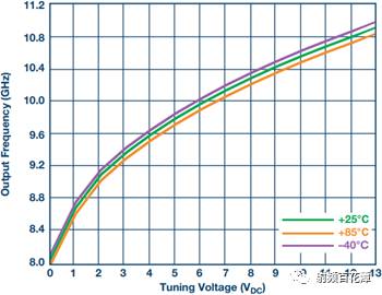
Figure 1. Traditional VCO - the relationship between tuning voltage and output frequency
The VCO architecture used in the integrated PLL/VCO solution is based on a traditional architecture, but it is quite different. The integrated PLL/VCO integrates multiple legacy VCOs to produce a very wide bandwidth VCO. Each VCO - created by accessing and disconnecting capacitors - is called a frequency band. The PLL and VCO are integrated on a single chip, enabling a multi-band architecture. Each time the user wishes to lock a new frequency, the device initiates a VCO calibration process. The chip quickly traverses the VCO band and selects a band that best fits the desired output frequency. Once the VCO band is selected, the PLL locks the loop and keeps the output at the desired frequency.
The first generation of PLL/VCO chips has more than 4 GHz bandwidth! In contrast, discrete solutions have only 100 MHz to 300 MHz bandwidth—and the 4 GHz frequency range is implemented by a tiny chip rather than the multiple PLLs, VCOs, filters, and switches that were previously required. Figure 2 shows the relationship between the tuning voltage and the output frequency of a multi-band PLL/VCO. In this example, the fundamental VCO output range is specified from 2200 MHz to 4400 MHz. The VCO output has a set of dividers, but it is still inside the chip and can split the signal down to a minimum of 35 MHz; this is what is achieved over the 4 GHz bandwidth – all from a single 5 mm × 5 mm package.
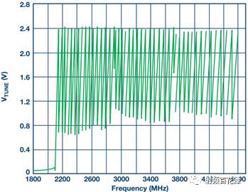
Figure 2. Multiband VCO - the relationship between tuning voltage and output frequency
While this breakthrough technology greatly increases the frequency range, reduces board space, cost and extra work, it still has shortcomings that make integration solutions not completely replace discrete solutions. The most important performance specifications for many applications (except the frequency range) are phase noise.
Why is phase noise so important? Imagine a system that transmits signals through clear air. Assume that the signal-to-noise ratio of the transmitted signal at the transmitting antenna is 50 dB. This means that the signal to be received by the receiver is 50 dB stronger than the noise on either side of the transmitted signal (ie adjacent higher and lower frequencies). Assuming that this signal can be transmitted for 10 miles, the signal power after that will decay into noise and the transmission will be lost. Now, assume that the phase noise of the frequency synthesizer is improved by 3 dB. This means that the transmitted signal has a signal-to-noise ratio of 53 dB. Therefore, the transmitted signal power is twice that of the previous 10 mile distance signal, and it can travel farther before it decays into noise. A farther transmission distance means fewer repeaters/transmitters are required and the cost is reduced.
In addition to this communication example, there is also a push for phase noise performance from the field of electronic test and measurement. Regardless of the phase noise performance required by the communications industry, the phase noise performance required for electronic test and measurement instruments will only be higher, in order to measure the communication protocol.
While many solutions can move from discrete to integrated – saving millions of dollars in process costs – the phase noise performance of the first generation PLL/VCO is not good enough for many low phase noise requirements. application. In addition to phase noise performance, the frequency range is quite low compared to many applications that require discrete PLLs and VCOs.
Frequency range issues can be solved with frequency multipliers and multipliers, but these are high power devices and increase the cost and board space of the solution.
Fortunately, with the introduction of these integrated solutions, the industry has embarked on the development of new IC processes to achieve the phase noise and frequency range improvements that are highly anticipated.
The stage at this time is ready for the debut of the second generation integrated PLL/VCO. The requirements for the second generation of products are as follows:
The output frequency is greater than 4.4 GHz.
Phase noise performance is comparable to discrete solutions.
Integrate PLLs and VCOs in a single small package.
The cost is lower than the discrete solution.
Later in 2014, the second generation of integrated PLL/VCO officially debuted. Products with more than 10 GHz output frequency range are beginning to appear on the market, with phase noise comparable to discrete VCOs in a 5 mm × 5 mm package at a lower price than similar discrete PLL and VCO solutions (but with a much narrower frequency range) .
For example, Analog Devices' ADF4355 series fulfills all the requirements of the second generation:
The output frequency ranges from 50 MHz to 13.6 GHz (one port ≤ 6.8 GHz and the other port ≤ 6.8 GHz).
Phase noise:
Traditional discrete VCOs at 10 GHz: –110 dBc/Hz (100 kHz offset) and –135 dBc/Hz (1 MHz offset). The discrete VCO uses a frequency range in exchange for phase noise performance.
The ADF4355 series is at 10 GHz: –106.5 dBc/Hz (100 kHz offset) and –130 dBc/Hz (1 MHz offset).
5 mm × 5 mm LFCSP package.
Prices vary from device to device, but at a lower cost than discrete solutions.
Now, users not only enjoy the phase noise performance benefits of discrete solutions, but they also get all the other benefits of an integrated solution. More advantageously, PLL technology has also evolved over the years, so the PLL performance of second-generation PLL/VCO devices has also improved.
For the first generation PLL/VCO, the maximum phase frequency detector (PFD) frequency of the PLL module is around 32 MHz, and the resolution of the fractional-N divider is around 12 bits. This combination means that the typical channel resolution is in the tens of kHz. The second-generation PLL/VCO has a maximum PFD frequency greater than 100 MHz, and the fractional-N divider has a resolution of 25 bits or even up to 49 bits. There are two main advantages to this - the higher the PFD frequency, the lower the PLL phase noise (for every doubling of the PFD frequency, the N divider can be halved and the N divider noise distribution is correspondingly reduced by 3 dB); Bits and even higher resolutions support precision frequency generation and sub-Hz frequency stepping (frequency resolution).
Spurious performanceThere is an important aspect to integrating PLL/VCO that needs to be discussed. One advantage of the discrete solution is pointed out above, that is, the physical isolation between the two chips reduces the cross-coupling between the PLL and the VCO, thereby reducing the power of the interfering spurious signals. When integrating PLLs and VCOs, spurious performance is inevitably degraded. Some devices on the market try to keep this performance down to a very low level, giving the PLL/VCO a surprisingly good spurious performance – the HMC830 is an example. Other PLL/VCO devices require additional measures to improve the level of spurs in order to support certain high performance products.
Change the PFD frequency to eliminate integer boundary spursOne technique is to use a frequency planning algorithm to change the PFD frequency of the PLL. This allows the spurious signals caused by the PFD module to be transferred to areas that do not have a large impact, thereby virtually eliminating spurs. For more information, see "Analyze, Optimize, and Eliminate Integer Boundary Spurious at Up to 13.6 GHz with Phase-Locked Loops for Integrated VCOs."
Isolate PLL and VCOAs mentioned above, the close proximity of the PLL and VCO circuits may cause unwanted coupling. To solve this problem, the PLL and VCO circuits can be physically isolated using a two-chip solution. This provides the benefits of a low spurious signal for a discrete solution and the wide output frequency advantage of an integrated solution.
The HMC704 from ADI's discrete fractional-N PLL product line is ideal for this task. In this solution, one of the VCO output signals (the ADF4355 series all have two outputs) is fed to the HMC704 (this signal uses an optional 10 dB attenuator to further reduce spurious levels). The ADF4355 PLL was originally used to complete the VCO calibration and lock the desired frequency. The ADF4355 PLL section can then be turned off, with the charge pump tri-stated and the counter held in reset, eliminating all spurs in the PLL, and the HMC704 will keep the loop locked. There are many advantages to doing this:
Using a PLL in a chip other than the VCO reduces spurious power.
The inherent spurious performance of the HMC704 is superior to the ADF4355 PLL - so the spurs are further reduced.
The HMC704's normalized phase noise floor is lower than the ADF4355 PLL – so the noise at the output of the frequency synthesizer is lower.
To close the loop, the HMC704 charge pump output is connected to a loop filter. The loop filter output must be connected to the ADF4355 VTUNE pin. When the loop is locked, the HMC704 is only used as a PLL and the ADF5355 is only used as a VCO. To completely eliminate spurious in the ADF4355 PLL, the ADF4355 reference input pin must be grounded when the ADF4355 PLL is not in use. Fortunately, this is easy to do in the HMC704. The HMC704 has a general purpose output (GPO) pin that can be directly connected to the ADF4355 reference input pin. When the ADF4355 requires a reference signal (for VCO calibration), the HMC704 can route its reference signal to the GPO pin; when it is not necessary to ground the ADF4355 reference input pin, the HMC704 can be set to output GND through the GPO pin. Figure 3 shows this circuit.
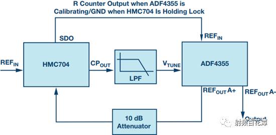
Figure 3. Using the external HMC704 PLL to lock the ADF4355 to improve spurious performance
Analog Devices has introduced four ADF4355 series, an important device with second-generation PLL/VCO performance. There are four devices in the series: three of them are very similar, with only a different frequency range; the fourth is a low-power version.
ADF4355-2: Integrated PLL/VCO with output from 53 MHz to 4400 MHz.
ADF4355: Integrated PLL/VCO with output from 53 MHz to 6800 MHz.
ADF5355: Integrated PLL/VCO with output from 53 MHz to 13,600 MHz.
ADF4355-3: Low power integrated PLL/VCO with output from 51 MHz to 6600 MHz.
Ningbo Autrends International Trade Co.,Ltd. , https://www.supervapebar.com